
Datasheet

TAS5614LA
www.ti.com
SLAS846 –MAY 2012
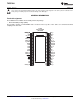
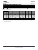
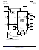
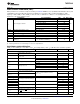
PIN FUNCTIONS
PIN NAME PINOUT DDV-44 I/O/P
(1)
DESCRIPTION
AVDD 13 P Internal voltage regulator, analog section
BST_A 44 P Bootstrap pin, A-side
BST_B 43 P Bootstrap pin, B-side
BST_C 24 P Bootstrap pin, C-side
BST_D 23 P Bootstrap pin, D-side
CLIP 18 O Clipping warning; open drain; active low
C_START 7 O Startup ramp
DVDD 8 P Internal voltage regulator, digital section
FAULT 16 O Shutdown signal, open drain; active low
9, 10, 11, 12, 25,
GND P Ground
26, 33, 34, 41, 42
GVDD_AB 1 P Gate-drive voltage supply; AB-side
GVDD_CD 22 P Gate-drive voltage supply; CD-side
INPUT_A 5 I PWM Input signal for half-bridge A
INPUT_B 6 I PWM Input signal for half-bridge B
INPUT_C 14 I PWM Input signal for half-bridge C
INPUT_D 15 I PWM Input signal for half-bridge D
M1 19 I Mode selection 1 (LSB)
M2 20 I Mode selection 2
M3 21 I Mode selection 3 (MSB)
OC_ADJ 3 O Over-Current threshold programming pin
OTW 17 O Over-temperature warning; open drain; active low
OUT_A 39, 40 O Output, half-bridge A
OUT_B 35 O Output, half-bridge B
OUT_C 32 O Output, half-bridge C
OUT_D 27, 28 O Output, half-bridge D
PVDD_AB 36, 37, 38 P PVDD supply for half-bridge A and B
PVDD_CD 29, 30, 31 P PVDD supply for half-bridge C and D
RESET 4 I Device reset Input; active low
VDD 2 P Input power supply
PowerPAD™ P Ground, connect to grounded heat sink
(1) I = Input, O = Output, P = Power
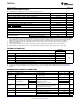
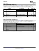
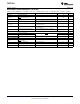
Table 1. ORDERING INFORMATION
(1)
T
A
PACKAGE DESCRIPTION
TAS5614LADDV
0°C–70°C 44 pin HTSSOP
TAS5614LADDVR
(1) For the most current package and ordering information, see the Package Option Addendum at the end of this document, or see the TI
website at www.ti.com.
Copyright © 2012, Texas Instruments Incorporated Submit Documentation Feedback 3
Product Folder Link(s): TAS5614LA