
Datasheet
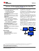

TAS5614LA
SLAS846 –MAY 2012
www.ti.com
ABSOLUTE MAXIMUM RATINGS
over operating free-air temperature range unless otherwise noted
(1)
TAS5614LA UNIT
VDD to GND, GVDD_X
(2)
to GND –0.3 to 13.2 V
PVDD_X
(2)
to GND
(3)
, OUT_X to GND
(3)
, BST_X to GVDD_X
(2)(3)
–0.3 to 50 V
BST_X to GND
(3)(4)
–0.3 to 62.5 V
DVDD to GND –0.3 to 4.2 V
AVDD to GND –0.3 to 8.5 V
OC_ADJ, M1, M2, M3, C_START, INPUT_X to GND –0.3 to 4.2 V
RESET, FAULT, OTW, CLIP, to GND –0.3 to 4.2 V
Maximum continuous sink current (FAULT, OTW, CLIP) 9 mA
Maximum operating junction temperature range, T
J
0 to 150 °C
Storage temperature, T
stg
–40 to 150 °C
Lead temperature 260 °C
Human body model
(4)
(all pins) ±2 kV
Electrostatic discharge
Charged device model
(4)
(all pins) ±500 V
(1) Stresses beyond those listed under Absolute Maximum Ratings may cause permanent damage to the device. These are stress ratings
only, and functional operation of the device at these or any other conditions beyond those indicated under Recommended Operating
Conditions is not implied. Exposure to absolute-maximum-rated conditions for extended periods may affect device reliability.
(2) GVDD_X and PVDD_X represents a full bridge gate drive or power supply. GVDD_X is GVDD_AB or GVDD_CD, PVDD_X is
PVDD_AB or PVDD_CD
(3) These voltages represents the DC voltage + peak AC waveform measured at the terminal of the device in all conditions.
(4) Maximum BST_X to GND voltage is the sum of maximum PVDD to GND and GVDD to GND voltages minus a diode drop.
THERMAL INFORMATION
TAS5614LA
THERMAL METRIC
(1)
UNITS
DDV (44-PIN)
θ
JH
Junction-to-heat sink thermal resistance
(2)
2.3
θ
JCtop
Junction-to-case (top) thermal resistance 0.8
θ
JB
Junction-to-board thermal resistance 2.1
°C/W
ψ
JT
Junction-to-top characterization parameter 0.8
ψ
JB
Junction-to-board characterization parameter 2.1
θ
JCbot
Junction-to-case (bottom) thermal resistance n/a
(1) For more information about traditional and new thermal metrics, see the IC Package Thermal Metrics application report, SPRA953.
(2) Thermal data are obtained with 85°C heat sink temperature using thermal compound with 0.7W/mK thermal conductivity and 2mil
thickness.
RECOMMENDED OPERATING CONDITIONS
MIN TYP MAX UNIT
PVDD_X Full-bridge supply DC supply voltage 12 36 38 V
Supply for logic regulators and gate-drive
GVDD_X DC supply voltage 10.8 12 13.2 V
circuitry
VDD Digital regulator supply voltage DC supply voltage 10.8 12 13.2 V
BTL 3.0 4.0
Output filter: L = 10 µH, 1 µF.
R
L
Load impedance SE Output AD modulation, 1.5 3.0 Ω
switching frequency > 350 kHz.
PBTL 1.5 2.0
Minimum inductance at overcurrent limit,
L
OUTPUT
Output filter inductance including inductor tolerance, temperature 5 μH
and possible inductor saturation
F
PWM
PWM frame rate 352 384 500 kHz
C
PVDD
PVDD close decoupling capacitors 0.44 1 μF
BTL and PBTL configuration 100 nF
C_START Startup ramp capacitor
SE and 1xBTL+2xSE configuration 1 μF
4 Submit Documentation Feedback Copyright © 2012, Texas Instruments Incorporated
Product Folder Link(s): TAS5614LA