
Datasheet
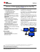

TAS5614LA
www.ti.com
SLAS846 –MAY 2012
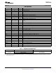
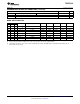
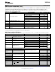
RECOMMENDED OPERATING CONDITIONS (continued)
MIN TYP MAX UNIT
R
OC
Over-current programming resistor Resistor tolerance = 5% 24 33 kΩ
R
OC_LATCHED
Over-current programming resistor Resistor tolerance = 5% 47 62 68 kΩ
T
J
Junction temperature 0 125 °C
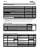
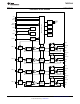
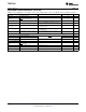
MODE SELECTION PINS
MODE PINS
PWM Input
(1)
Output Configuration Input A Input B Input C Input D MODE
M3 M2 M1
0 0 0 2N + 1 2 x BTL PWMa PWMb PWMc PWMd AD Mode
0 0 1 1N + 1
(2)
2 x BTL PWMa Unused PWMc Unused AD Mode
0 1 0 2N + 1 2 x BTL PWMa PWMb PWMc PWMd BD Mode
0 1 1 1N + 1
(2)
1 x BTL + 2 x SE PWMa Unused PWMc PWMd AD Mode
1 0 0 2N + 1 1 x PBTL PWMa PWMb 0 0 AD Mode
1 0 0 1N + 1
(2)
1 x PBTL PWMa Unused 0 1 AD Mode
1 0 0 2N + 1 1 x PBTL PWMa PWMb 1 0 BD Mode
1 0 1 1N + 1 4 x SE
(3)
PWMa PWMb PWMc PWMd AD Mode
(1) The 1N and 2N naming convention is used to indicate the number of PWM lines to the power stage per channel in a specific mode.
(2) Using 1N interface in BTL and PBTL mode results in increased DC offset on the output terminals.
(3) The 4xSE mode can be used as 1xBTL + 2xSE configuration by feeding a 2N PWM signal to either INPUT_AB or INPUT_CD for
improved DC offset accuracy
Copyright © 2012, Texas Instruments Incorporated Submit Documentation Feedback 5
Product Folder Link(s): TAS5614LA