
Datasheet
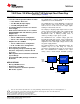

TAS5614LA
www.ti.com
SLAS846 –MAY 2012
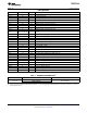
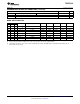
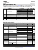
AUDIO SPECIFICATION MONO (PBTL)
Audio performance is recorded as a chipset consisting of a TASxxxx PWM Processor (modulation index limited to 97.7%) and
a TAS5614LA power stage with PCB and system configurations in accordance with recommended guidelines. Audio
frequency = 1kHz, PVDD_X = 36V, GVDD_X = 12V, R
L
= 4Ω, f
S
= 384kHz, R
OC
= 24kΩ, T
C
= 75°C, Output Filter: L
DEM
=
10μH, C
DEM
= 1μF, unless otherwise noted.
PARAMETER TEST CONDITIONS MIN TYP MAX UNIT
R
L
= 2 Ω, 10%, THD+N 300
R
L
= 3 Ω, 10% THD+N 200
R
L
= 4 Ω, 10% THD+N 160
P
O
Power output per channel W
R
L
= 2 Ω, 1% THD+N 250
R
L
= 3 Ω, 1% THD+N 160
R
L
= 4 Ω, 1% THD+N 130
THD+N Total harmonic distortion + noise 1 W, 1 kHz signal 0.025 %
V
n
Output integrated noise A-weighted, AES17 measuring filter 180 μV
V
OS
Output offset voltage No signal 10 20 mV
SNR Signal to noise ratio
(1)
A-weighted, AES17 measuring filter 105 dB
DNR Dynamic range A-weighted, –60 dBFS (rel 1% THD) 105 dB
Power dissipation due to idle losses
P
idle
P
O
= 0, All channels switching
(2)
1.6 W
(IPVDD_X)
(1) SNR is calculated relative to 1% THD-N output level.
(2) Actual system idle losses are affected by core losses of output inductors.
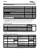
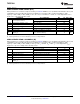
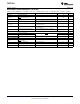
ELECTRICAL CHARACTERISTICS
PVDD_X = 36 V, GVDD_X = 12 V, VDD = 12 V, T
C
(Case temperature) = 75°C, f
S
= 384 kHz, unless otherwise specified.
PARAMETER TEST CONDITIONS MIN TYP MAX UNIT
INTERNAL VOLTAGE REGULATOR AND CURRENT CONSUMPTION
Voltage regulator, only used as a
DVDD VDD = 12 V 3.0 3.3 3.6 V
reference node
Voltage regulator, only used as a
AVDD VDD = 12 V 7.8 V
reference node
Operating, 50% duty cycle 20
I
VDD
VDD supply current mA
Idle, reset mode 20
50% duty cycle 9
I
GVDD_X
Gate-supply current per full-bridge mA
Reset mode 2
50% duty cycle without load 23
I
PVDD_X
Full-bridge idle current RESET low 1.9 mA
VDD and GVDD_X at 0V 0.35
OUTPUT-STAGE MOSFETs
Drain-to-source resistance, low side
R
DS(on), LS
60 100 mΩ
(LS)
T
J
= 25°C, excludes metalization resistance,
GVDD = 12 V
Drain-to-source resistance, high side
R
DS(on), HS
60 100 mΩ
(HS)
I/O PROTECTION
V
uvp,GVDD
8.5 V
Undervoltage protection limit, GVDD_X
V
uvp,GVDD, hyst
(1)
0.7 V
V
uvp,VDD
8.5 V
Undervoltage protection limit, VDD
V
uvp,VDD, hyst
(1)
0.7 V
V
uvp,PVDD
8.5 V
Undervoltage protection limit, PVDD_X
V
uvp,PVDD,hyst
(1)
0.7 V
OTW
(1)
Overtemperature warning 115 125 135 °C
Temperature drop needed below OTW
OTW
hyst
(1)
temperature for OTW to be inactive 25 °C
after OTW event.
OTE
(1)
Overtemperature error 145 155 165 °C
(1) Specified by design.
Copyright © 2012, Texas Instruments Incorporated Submit Documentation Feedback 9
Product Folder Link(s): TAS5614LA