
Datasheet


Table Of Contents
- FEATURES
- DESCRIPTION/ORDERING INFORMATION
- DESCRIPTION/ORDERING INFORMATION (CONTINUED)
- ABSOLUTE MAXIMUM RATINGS
- RECOMMENDED OPERATING CONDITIONS
- ELECTRICAL CHARACTERISTICS
- I2C INTERFACE TIMING REQUIREMENTS
- RESET TIMING REQUIREMENTS
- SWITCHING CHARACTERISTICS
- TYPICAL CHARACTERISTICS
- PARAMETER MEASUREMENT INFORMATION
- APPLICATION INFORMATION
- REVISION HISTORY
ADDR
P20
P21
P22
P23
P24
P25
P26
P27
RESET
P00
P01
P02
P03
P04
P05
P06
P07
V
CCI
GND
INT
V
CCP
SDA
P17
P16
P15
P14
P13
P10
P11
P12
SCL
1
2
3
4
5
6
7
8
25
26
27
29
28
30
31
32
16
15
14
13
9
10
11
12
18
17
24
23
22
21
20
19
Exposed
Center Pad
TCA6424A
www.ti.com
SCPS193B –JULY 2010–REVISED SEPTEMBER 2010
LOW-VOLTAGE 24-BIT I
2
C AND SMBus I/O EXPANDER
WITH INTERRUPT OUTPUT, RESET, AND CONFIGURATION REGISTERS
Check for Samples: TCA6424A
1
FEATURES
• Operating Power-Supply Voltage Range of • Polarity Inversion Register
1.65 V to 5.5 V
• Internal Power-On Reset
• Allows Bidirectional Voltage-Level Translation
• Power Up With All Channels Configured as
and GPIO Expansion Between:
Inputs
– 1.8-V SCL/SDA and
• No Glitch On Power Up
1.8-V, 2.5-V, 3.3-V, or 5-V P Port
• Noise Filter on SCL/SDA Inputs
– 2.5-V SCL/SDA and
• Latched Outputs With High-Current Drive
1.8-V, 2.5-V, 3.3-V, or 5-V P Port
Maximum Capability for Directly Driving LEDs
– 3.3-V SCL/SDA and
• Latch-Up Performance Exceeds 100 mA Per
1.8-V, 2.5-V, 3.3-V, or 5-V P Port
JESD 78, Class II
– 5-V SCL/SDA and
• ESD Protection Exceeds JESD 22
1.8-V, 2.5-V, 3.3-V, or 5-V P Port
– 2000-V Human-Body Model (A114-A)
• I
2
C to Parallel Port Expander
– 200-V Machine Model (A115-A)
• Low Standby Current Consumption of 1 mA
– 1000-V Charged-Device Model (C101)
• Schmitt-Trigger Action Allows Slow Input
Transition and Better Switching Noise
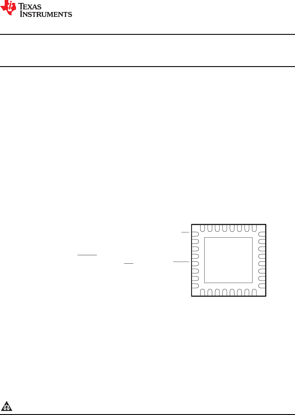
RGJ/RSM PACKAGE
(BOTTOM VIEW)
Immunity at the SCL and SDA Inputs
– V
hys
= 0.18 V Typ at 1.8 V
– V
hys
= 0.25 V Typ at 2.5 V
– V
hys
= 0.33 V Typ at 3.3 V
– V
hys
= 0.5 V Typ at 5 V
• 5-V Tolerant I/O Ports
• Active-Low Reset Input (RESET)
• Open-Drain Active-Low Interrupt Output (INT)
• 400-kHz Fast I
2
C Bus
• Input/Output Configuration Register
If used, the exposed center pad must be
connected as a secondary ground or left
electrically open.
DESCRIPTION/ORDERING INFORMATION
This 24-bit I/O expander for the two-line bidirectional bus (I
2
C) is designed to provide general-purpose remote I/O
expansion for most microcontroller families via the I
2
C interface [serial clock (SCL) and serial data (SDA)].
The major benefit of this device is its wide V
CC
range. It can operate from 1.65 V to 5.5 V on the P-port side and
on the SDA/SCL side. This allows the TCA6424A to interface with next-generation microprocessors and
microcontrollers on the SDA/SCL side, where supply levels are dropping down to conserve power. In contrast to
the dropping power supplies of microprocessors and microcontrollers, some PCB components, such as LEDs,
remain at a 5-V power supply.
1
Please be aware that an important notice concerning availability, standard warranty, and use in critical applications of Texas
Instruments semiconductor products and disclaimers thereto appears at the end of this data sheet.
PRODUCTION DATA information is current as of publication date.
Copyright © 2010, Texas Instruments Incorporated
Products conform to specifications per the terms of the Texas
Instruments standard warranty. Production processing does not
necessarily include testing of all parameters.