
OWNERS MANUAL Telephone TCM4300

4–29
4.24 Microcontroller Interface
The microcontroller interface of the TCM4300 is a general purpose bus interface (see Table 4–24) which
ensures compatibility with a wide range of microcontrollers, including the Mitsubshi M37700 series and most
Intel and Motorola series. The interface consists of a pair of microcontroller type select inputs MTS1 and
MTS0, address and data buses, as well as several input and output control signals that are designed to
operate in a manner compatible with the microcontroller selected by the user. See Sections 3.2 to 3.11 for
Interface timing requirements.
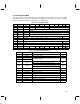
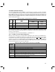
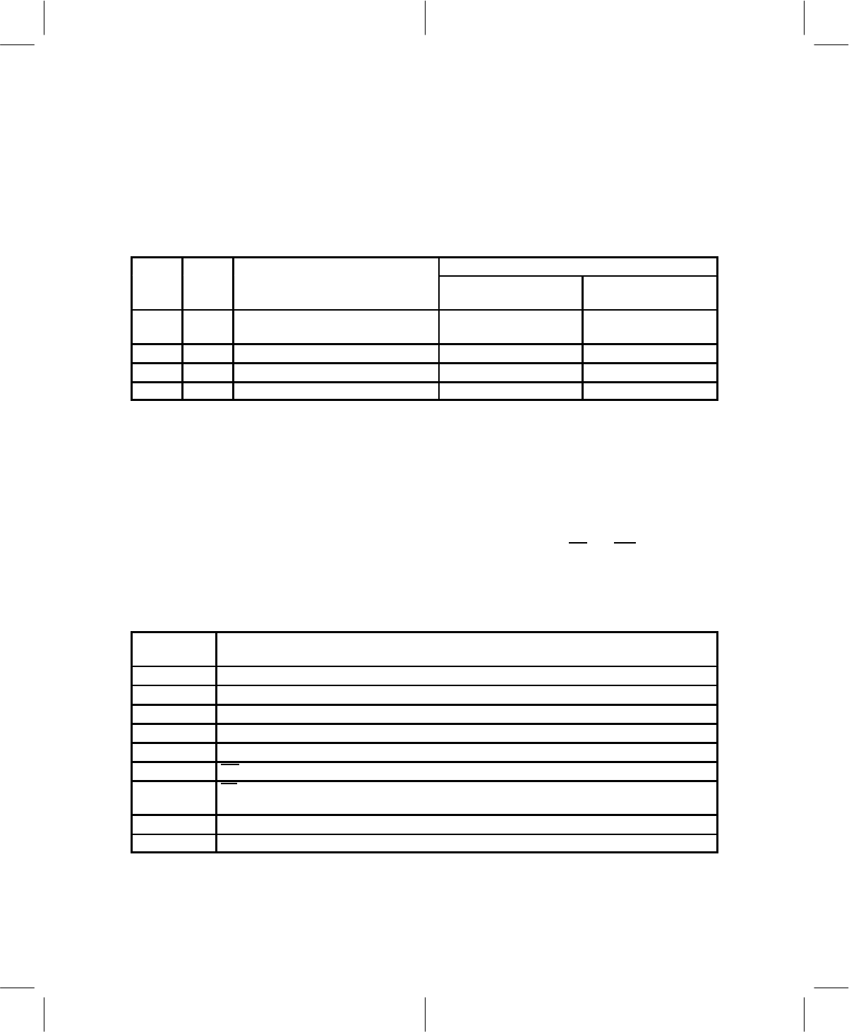
Table 4–24. Microcontroller Interface Configuration
MTS1
MTS0
MODE
POLARITY
MTS1 MTS0 MODE
DATA STROBE (DS)
ACTIVE
INTERRUPT/OUTPUT
ACTIVE
0 0 Intel
Low
(separate read and write)
High
1 0 Motorola 16-bit and Mitsubishi Low Low
0 1 Motorola 8-bit High Low
1 1 Reserved N/A N/A
The microcontroller interface of the TCM4300 is designed to allow direct connection to many
microcontrollers. Except for the interrupt terminals, it is designed to connect to microcontrollers in the same
manner as a memory device.
The internal chip select is asserted when MCCSH = 1 and MCCSL = 0.
4.24.1 Intel Microcontroller Mode Of Operation
When the microcontroller type select inputs MTS1 and MTS0 are both held low, the TCM4300 micro-
controller interface is configured into Intel mode (see Table 4-25). In this mode, the interface uses separate
read and write control strobes and active-high interrupt signals. The processor RD
and WR strobe signals
should be connected to the TCM4300 MCDS signal and MCRW signal, respectively. The multiplexed
address and data buses of the microcontroller must be demultiplexed by external hardware. Table 4–25 lists
the microcontroller interface connections for Intel mode.
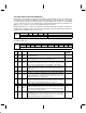
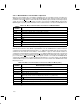
Table 4–25. Microcontroller Interface Connections for Intel Mode
TCM4300
TERMINAL
MICROCONTROLLER TERMINAL
MTS1, MTS0 Tie to logic level low
MCCSH Not on microcontroller; can be used for address decoding
MCCSL Not on microcontroller; can be used for address decoding
MCD7–MCD0 AD[7:0] data bus on microcontroller
MCA4–MCA0 Demultiplexed address bits not on microcontroller
MCRW WR (Active-low write data strobe)
MCDS RD (Active-low read data strobe) MCDS configured to active-low operation by MTS1 and MTS0. The
microcontroller bus must be demultiplexed by external hardware.
MWBDFINT Either one of INT3 through INT0 as appropriate
DINT Either one of INT3 through INT0 as appropriate