THS4012 Dual High Speed Operational Amplifier Evaluation Module User’s Guide May 1999 Mixed-Signal Products SLOU041
IMPORTANT NOTICE Texas Instruments (TI) reserves the right to make changes to its products or to discontinue any semiconductor product or service without notice, and advises its customers to obtain the latest version of relevant information to verify, before placing orders, that the information being relied on is current. TI warrants performance of its semiconductor products and related software to the specifications applicable at the time of sale in accordance with TI’s standard warranty.
Preface Related Documentation From Texas Instruments J THS4012 DUAL LOW-NOISE HIGH-SPEED OPERATIONAL AMPLIFIER (literature number SLOS216) This is the data sheet for the THS4012 operational amplifier integrated circuit that is used in the THS4012 evaluation module. FCC Warning This equipment is intended for use in a laboratory test environment only.
iv
Running Title—Attribute Reference Contents 1 General . . . . . . . . . . . . . . . . . . . . . . . . . . . . . . . . . . . . . . . . . . . . . . . . . . . . . . . . . . . . . . . . . . . . . . . . . 1-1 1.1 Feature Highlights . . . . . . . . . . . . . . . . . . . . . . . . . . . . . . . . . . . . . . . . . . . . . . . . . . . . . . . . . . 1-2 1.2 Description . . . . . . . . . . . . . . . . . . . . . . . . . . . . . . . . . . . . . . . . . . . . . . . . . . . . . . . . . . . . . . . . 1-3 1.
Running Title—Attribute Reference Figures 1–1 1–2 1–3 1–4 1–5 1–6 1–7 1–8 1–9 THS4012 Evaluation Module . . . . . . . . . . . . . . . . . . . . . . . . . . . . . . . . . . . . . . . . . . . . . . . . . . . 1-3 THS4012 EVM Schematic — Noninverting Operation . . . . . . . . . . . . . . . . . . . . . . . . . . . . . . 1-4 THS4012 EVM Schematic — Inverting Operation . . . . . . . . . . . . . . . . . . . . . . . . . . . . . . . . . 1-7 THS4012 EVM Schematic — Differential Input (Noninverting Operation) . . . .
Chapter 1 General This chapter details the Texas Instruments (TI) THS4012 dual high-speed operational amplifier evaluation module (EVM), SLOP230. It includes a list of EVM features, a brief description of the module illustrated with a pictorial and a schematic diagram, EVM specifications, details on connecting and using the EVM, and discussions on high-speed amplifier design and thermal considerations. Topic Page 1.1 Feature Highlights . . . . . . . . . . . . . . . . . . . . . . . . . . . . . . . . .
Feature Highlights 1.
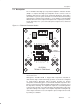
Description 1.2 Description The TI THS4012 dual high-speed operational amplifier evaluation module (EVM) is a complete dual high-speed amplifier circuit. It consists of the TI THS4012 dual low-noise high-speed operational amplifier IC, along with a small number of passive parts, mounted on a small circuit board measuring approximately 1.9 inch by 2.2 inch (Figure 1–1).
THS4012 EVM Noninverting Operation 1.3 THS4012 EVM Noninverting Operation The THS4012 EVM is shipped preconfigured for dual-channel noninverting operation, as shown in Figure 1–2. Note that compensation capacitors C3 and C6 are not installed. Figure 1–2. THS4012 EVM Schematic — Noninverting Operation C3 x µF J2 –VCC GND +VCC 1 –VCC 2 3 C2 6.8 µF C1 6.8 µF +VCC R5 1 kΩ R6 1 kΩ 2 +VCC C5 0.1 µF 8 U1:A THS4012 – J1 R7 49.9 Ω J3 Vout1 1 Vin1 R1 49.9 Ω R3 0Ω 3 + C4 0.
THS4012 EVM Noninverting Operation Any of the resistors on the EVM board can be replaced with a resistor of a different value; however, care must be taken because the surface-mount solder pads on the board are somewhat fragile and will not survive many desoldering/soldering operations. External factors can significantly affect the effective gain of the EVM.
Using the THS4012 EVM In The Noninverting Mode 1.4 Using the THS4012 EVM In The Noninverting Mode The THS4012 EVM operates from power-supply voltages ranging from ± 5 V to ± 15 V. As shipped, the EVM is configured for inverting operation and the gain is set to 4. Signal inputs on the module are terminated for 50-Ω nominal source impedance. An oscilloscope is typically used to view and analyze the EVM output signal.
THS4012 EVM Inverting Operation 1.5 THS4012 EVM Inverting Operation Although the THS4012 EVM is shipped preconfigured for dual-channel noninverting operation, it can be reconfigured for inverting operation by making the following component changes: 1) Move resistor R3 to the R2 location and R5 to the R4 location on the board. 2) Move resistor R11 to the R10 location and R13 to the R12 location on the board. This configuration is shown in Figure 1–3.
THS4012 EVM Inverting Operation The gain of the EVM can easily be changed to support a particular application by changing the ratio of resistors R6 and R4 (channel 1) and R14 and R12 (channel 2) as described in the following equation: Inverting Gain F + –R + –RR46 R G and –R14 R12 In addition, some applications, such as those for video, may require the use of 75-Ω cable and 75-Ω EVM input termination and output isolation resistors.
Using the THS4012 EVM In The Inverting Mode 1.6 Using the THS4012 EVM In The Inverting Mode The THS4012 EVM operates from power-supply voltages ranging from ± 5 V to ± 15 V. As shipped, the EVM is configured for inverting operation. Move the resistors as detailed above to configure the EVM for noninverting operation, which sets the gain to –3. Signal inputs on the module are terminated for 50-Ω nominal source impedance. An oscilloscope is typically used to view and analyze the EVM output signal.
THS4012 EVM Differential Input 1.7 THS4012 EVM Differential Input The THS4012 EVM is shipped preconfigured for dual-channel, single-ended noninverting operation. It can be reconfigured for single-channel, differential operation, either noninverting or inverting. 1.7.1 Differential Input, Noninverting Operation Configure the THS4012 EVM for differential noninverting operation by removing two resistors and adding a resistor on the board: 1) Remove resistors R1 and R9.
THS4012 EVM Differential Input The gain of the EVM can easily be changed to support a particular application by simply changing the ratio of resistors R6 and R5 (channel 1) and R14 and R13 (channel 2) as described in the following equation: Noninverting Gain + 1 ) RRF + 1 ) RR65 G and 1 ) RR14 13 In addition, some applications, such as those for video, may require the use of 75-Ω cable and 75-Ω EVM input termination and output isolation resistors.
THS4012 EVM Differential Input Figure 1–5. THS4012 EVM Schematic — Differential Input (Inverting Operation) C3 x µF J2 –VCC GND +VCC 1 –VCC 2 3 C2 6.8 µF C1 6.8 µF +VCC R6 1 kΩ +VCC R4 1 kΩ J1 2 Vin1 – 8 C5 0.1 µF U1:A THS4012 R7 49.9 Ω J3 Vout1 1 3 + C4 0.1 µF 4 R2 0Ω C6 x µF –VCC R8 100 Ω R14 1 kΩ R12 1 kΩ J4 6 Vin2 5 – U1:B THS4012 + R15 49.
THS4012 EVM Differential Input Any resistor on the EVM board can be replaced with a resistor of a different value; however, care must be taken because the surface-mount solder pads on the board are somewhat fragile and will not survive many desoldering/soldering operations. External factors can significantly affect the effective gain of the EVM.
Using the THS4012 EVM With Differential Inputs 1.8 Using the THS4012 EVM With Differential Inputs The THS4012 EVM operates from power-supply voltages ranging from ± 5 V to ± 15 V. Move resistors on the board as detailed above for either noninverting or inverting operation to configure the EVM for differential input operation. Signal inputs on the module are terminated for 50-Ω nominal source impedance. An oscilloscope is typically used to view and analyze the EVM output signal.
THS4012 EVM Performance 1.10 THS4012 EVM Performance Figure 1–6 shows the typical frequency response of the THS4012 EVM using the noninverting configuration (G = 2). Typical – 0.1 dB bandwidth is 25 MHz and – 3-dB bandwidth is 75 MHz with both a ±15-V power supply and a ±5-V power supply. Figure 1–6. THS4012 EVM Frequency Response with Gain = 2 7 6 Output Amplitude – dB 5 4 3 2 1 VCC = ±5 V and ± 15 V VO = 0.
General High-Speed Amplifier Design Considerations 1.11 General High-Speed Amplifier Design Considerations The THS4012 EVM layout has been designed and optimized for use with high-speed signals and can be used as an example when designing THS4012 applications. Careful attention has been given to component selection, grounding, power supply bypassing, and signal path layout.
General PowerPAD Design Considerations 1.12 General PowerPAD Design Considerations The THS4012DGN IC is mounted in a special package incorporating a thermal pad that transfers heat from the IC die directly to the PCB. The PowerPAD package is constructed using a downset leadframe. The die is mounted on the leadframe but is electrically isolated from it. The bottom surface of the lead frame is exposed as a metal thermal pad on the underside of the package and makes physical contact with the PCB.
General PowerPAD Design Considerations 8) With these preparatory steps in place, the THS4012DGN IC is simply placed in position and run through the solder reflow operation as any standard surface-mount component. This results in a part that is properly installed. The actual thermal performance achieved with the THS4012DGN in its PowerPAD package depends on the application.
General PowerPAD Design Considerations Correct PCB layout and manufacturing techniques are critical for achieving adequate transfer of heat away from the PowerPAD IC package. More details on proper board layout can be found in the THS4012 Low-noise Dual Differential Receiver data sheet (SLOS216). For more general information on the PowerPAD package and its thermal characteristics, see the Texas Instruments Technical Brief, PowerPAD Thermally Enhanced Package (SLMA002).
1-20 General
Chapter 2 Reference This chapter includes a complete schematic, parts list, and PCB layout illustrations for the THS4012 EVM. Topic Page 2.1 THS4012 EVM Complete Schematic . . . . . . . . . . . . . . . . . . . . . . . . . . . . 2–2 2.1 THS4012 Dual High-Speed Operational Amplifier EVM Parts List . . 2–3 2.2 THS4012 EVM Board Layouts . . . . . . . . . . . . . . . . . . . . . . . . . . . . . . . . . .
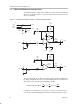
THS4012 EVM Complete Schematic 2.1 THS4012 EVM Complete Schematic Figure 2–1 shows the complete THS4012 EVM schematic. The EVM is shipped preconfigured for dual-channel, single-ended inverting operation. Components showing a value of X are not supplied on the board, but can be installed by the user to reconfigure the EVM for noninverting and/or differential operation. Figure 2–1. THS4012 EVM Schematic C3 x µF J2 –VCC GND +VCC 1 –VCC 2 3 C1 6.8 µF C2 6.
THS4012 Dual High-Speed Operational Amplifier EVM Parts List 2.2 THS4012 Dual High-Speed Operational Amplifier EVM Parts List Table 2–1. THS4012 EVM Parts List Reference Description Size Manufacturer/Supplier Part Number C1, C2 Capacitor, 6.8 µF, 35 V, Tantalum, SM C4, C5 Capacitor, 0.1 µF, Ceramic, 10%, SM J2 3-Pin Terminal Block (On Shore Tech.) Digi-Key ED1515–ND J1, J3, J4, J5 Connector, SMA 50-Ω vertical PC mount, throughhole Amphenol ARF1205–ND R1, R7, R9, R15 Resistor, 49.
THS4012 EVM Board Layouts 2.3 THS4012 EVM Board Layouts Board layout examples of the THS4012 EVM PCB are shown in the following illustrations. They are not to scale and appear here only as a reference. Figure 2–2.
THS4012 EVM Board Layouts Figure 2–3.
THS4012 EVM Board Layouts Figure 2–4.