
- Texas Instrumernts User's GuideTHS4503EVM


EVM Default Configuration
1-3
Introduction and Description
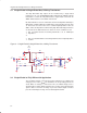
1.4 EVM Default Configuration
As delivered, the EVM has a fully functional example circuit, just add power
supplies, a signal source, and monitoring instrument. See Figure 1−1 for the
default schematic diagram. The user can change the gain by changing the
ratios of the feedback and gain resistors (see the device data sheet for
recommended resistor values). Chapter 5 has a complete EVM schematic
diagram showing all component locations.
The default configuration assumes a 50-Ω signal source and contains a
termination resistor R1 for the source.
Some components such as C8, C9, C11, C12, TP1, TP2, R10, T1, and J4 are
omitted on the application schematics of Chapter 3 for clarity.
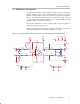
Figure 1−1. Schematic of the Populated Circuit on the EVM (Default Configuration)
J6
Vin+
+VS
+VS
R8
340
Ω
J2
Vout+
R10
280
Ω
R7 0
R4
392
Ω
TP4
C2 0
+
C8
6.8
µ
F
−VS
C12
0.1
µ
F
−
Vocm
+
U1
THS4503
1
8
2
3
6
5
4
R5
392
Ω
R3
402
Ω
R2
374
Ω
J1
Vin−
J8
+VS
R9
340
Ω
J5
−VS
TP2
PD−
R1
56.2
Ω
TP1
Vocm
J7
GND
C9
0.1
µ
F
R17
0
J4
Vout
C1 0
TP5TP3
J3
Vout−
+
C11
6.8
µ
F
R6 0
T1
ADP4−1WT
6 1
5
4 3
−VS
C13
1
µ
F