
Datasheet
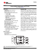


THS7320
SBOS565B –JULY 2011–REVISED SEPTEMBER 2012
www.ti.com
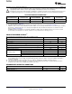
ELECTRICAL CHARACTERISTICS: V
S+
= 3 V, Video Section (continued)
At T
A
= +25°C, load = 150 Ω || 6.2 pF to GND, and dc-coupled input and output, unless otherwise noted.
THS7320IYHC
TEST
PARAMETER CONDITIONS MIN TYP MAX UNIT LEVEL
(1)
POWER SUPPLY (V
S+
)
Operating Voltage V
S+
2.5 3 5.5 V B
Video enable pin = 1.8 V, no load, V
IN
= 0 V 2.7 3.5 4.7 mA A
V
S+
total quiescent current
Video enable pin = 0 V, no load, V
IN
= 0 V 0.15 1 µA A
V
S+
power-supply rejection ratio
At dc 44 50 dB A
(PSRR)
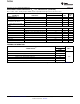
VIDEO ENABLE LOGIC CHARACTERISTICS
V
IH
Enabled 1.17 V A
V
IL
Disabled 0.4 V A
I
IH
Enable pin = 1.8 V, current flows into the pin 1.8 3 µA A
I
IH
Enable pin = 3 V, current flows into the pin 3 5 µA A
I
IL
Enable pin = 0 V, current flows into the pin –0.01 –0.5 µA A
Input resistance 1 MΩ C
Disable time 130 ns C
Enable time 120 ns C
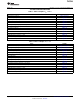
THERMAL INFORMATION
THS7320IYHC
THERMAL METRIC
(1)
YHC UNITS
9 PINS
θ
JA
Junction-to-ambient thermal resistance 159.3
θ
JCtop
Junction-to-case (top) thermal resistance 2.2
θ
JB
Junction-to-board thermal resistance 2.4
°C/W
ψ
JT
Junction-to-top characterization parameter 8.9
ψ
JB
Junction-to-board characterization parameter 88.4
θ
JCbot
Junction-to-case (bottom) thermal resistance n/a
(1) For more information about traditional and new thermal metrics, see the IC Package Thermal Metrics application report, SPRA953.
4 Submit Documentation Feedback Copyright © 2011–2012, Texas Instruments Incorporated
Product Folder Links: THS7320