
Datasheet


SLOS078J − NOVEMBER 1978 − REVISED SEPTEMBER 2004
1
POST OFFICE BOX 655303 • DALLAS, TEXAS 75265
D Very Low Power Consumption
D Typical Supply Current . . . 200 µA
(Per Amplifier)
D Wide Common-Mode and Differential
Voltage Ranges
D Low Input Bias and Offset Currents
D Common-Mode Input Voltage Range
Includes V
CC+
D Output Short-Circuit Protection
D High Input Impedance . . . JFET-Input Stage
D Internal Frequency Compensation
D Latch-Up-Free Operation
D High Slew Rate . . . 3.5 V/µs Typ
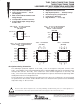
1
2
3
4
8
7
6
5
OFFSET N1
IN−
IN+
V
CC−
NC
V
CC+
OUT
OFFSET N2
TL061, TL061A . . . D, P, OR PS PACKAGE
TL061B ...P PACKAGE
(TOP VIEW)
1
2
3
4
8
7
6
5
1OUT
1IN−
1IN+
V
CC−
V
CC+
2OUT
2IN−
2IN+
TL062 . . . D, JG, P, PS, OR PW PACKAGE
TL062A . . . D, P, OR PS PACKAGE
TL062B ...D OR P PACKAGE
(TOP VIEW)
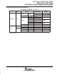
1
2
3
4
5
6
7
14
13
12
11
10
9
8
1OUT
1IN−
1IN+
V
CC+
2IN+
2IN−
2OUT
4OUT
4IN−
4IN+
V
CC−
3IN+
3IN−
3OUT
TL064 . . . D, J, N, NS, PW, OR W PACKAGE
TL064A, TL064B ...D OR N PACKAGE
(TOP VIEW)
NC − No internal connection
NC
2OUT
NC
2IN−
NC
3 2 1 20 19
910111213
4
5
6
7
8
18
17
16
15
14
NC
1IN−
NC
1IN+
NC
TL062 . . . FK PACKAGE
(TOP VIEW)
NC
1OUT
NC
2IN+
NC
NC
NC
NC
V
CC−
V
CC+
3212019
910111213
4
5
6
7
8
18
17
16
15
14
4IN+
NC
V
CC−
NC
3IN+
1IN+
NC
V
CC+
NC
2IN+
1IN−
1OUT
NC
3
OUT
3IN−
4OUT
4IN−
2IN−
2
OUT
NC
TL064 . . . FK PACKAGE
(TOP VIEW)
description/ordering information
The JFET-input operational amplifiers of the TL06_ series are designed as low-power versions of the
TL08_ series amplifiers. They feature high input impedance, wide bandwidth, high slew rate, and low input offset
and input bias currents. The TL06_ series features the same terminal assignments as the TL07_ and
TL08_ series. Each of these JFET-input operational amplifiers incorporates well-matched, high-voltage JFET
and bipolar transistors in an integrated circuit.
The C-suffix devices are characterized for operation from 0°C to 70°C. The I-suffix devices are characterized
for operation from −40°C to 85°C, and the M-suffix devices are characterized for operation over the full military
temperature range of −55°C to 125°C.
Please be aware that an important notice concerning availability, standard warranty, and use in critical applications o
f
Texas Instruments semiconductor products and disclaimers thereto appears at the end of this data sheet.
Copyright 2004, Texas Instruments Incorporated
!" # $%&" !# '%()$!" *!"&+
*%$"# $ " #'&$$!"# '& ",& "&# &-!# #"%&"#
#"!*!* .!!"/+ *%$" '$&##0 *&# " &$&##!)/ $)%*&
"&#"0 !)) '!!&"&#+
'*%$"# $')!" " 12313 !)) '!!&"&# !& "&#"&*
%)&## ",&.#& "&*+ !)) ",& '*%$"# '*%$"
'$&##0 *&# " &$&##!)/ $)%*& "&#"0 !)) '!!&"&#+