
Datasheet


SLVS024E – FEBRUARY 1983 – REVISED NOVEMBER 1999
1
www.ti.com
D Complete PWM Power Control Circuitry
D Completely Synchronized Operation
D Internal Undervoltage Lockout Protection
D Wide Supply Voltage Range
D Internal Short-Circuit Protection
D Oscillator Frequency ...500 kHz Max
D Variable Dead Time Provides Control Over
Total Range
D Internal Regulator Provides a Stable 2.5-V
Reference Supply
D Available in Q-Temp Automotive
HighRel Automotive Applications
Configuration Control / Print Support
Qualification to Automotive Standards
description
The TL1451A incorporates on a single monolithic
chip all the functions required in the construction
of two pulse-width-modulation (PWM) control
circuits. Designed primarily for power-supply
control, the TL1451A contains an on-chip 2.5-V
regulator, two error amplifiers, an adjustable
oscillator, two dead-time comparators, undervol-
tage lockout circuitry, and dual common-emitter
output transistor circuits.
The uncommitted output transistors provide
common-emitter output capability for each
controller. The internal amplifiers exhibit a common-mode voltage range from 1.04 V to 1.45 V. The dead-time
control (DTC) comparator has no offset unless externally altered and can provide 0% to 100% dead time. The
on-chip oscillator can be operated by terminating RT and CT. During low V
CC
conditions, the undervoltage
lockout control circuit feature locks the outputs off until the internal circuitry is operational.
The TL1451AC is characterized for operation from –20°C to 85°C. The TL1451AQ is characterized for operation
from –40°C to 125°C. The TL1451AM is characterized for operation from –55°C to 125°C.
AVAILABLE OPTIONS
PACKAGED DEVICES
T
A
SMALL
OUTLINE
(D)
SMALL
OUTLINE
(DB)
†
PLASTIC DIP
(N)
SMALL
OUTLINE
(NS)
TSSOP
(PW)
†
CHIP
CARRIER
(FK)
CERAMIC
DIP
(J)
–20°C to 85°C TL1451ACD TL1451ACDB TL1451ACN TL1451ACNS TL1451ACPW — —
–40°C to 125°C TL1451AQD — — — — — —
–55°C to 125°C — — — — — TL1451AMFK TL1451AMJ
†
The DB and PW packages are only available left-end taped and reeled (add LE suffix, i.e., TL1451ACPWLE).
Copyright 1999, Texas Instruments Incorporated
Please be aware that an important notice concerning availability, standard warranty, and use in critical applications of
Texas Instruments semiconductor products and disclaimers thereto appears at the end of this data sheet.
1
2
3
4
5
6
7
8
16
15
14
13
12
11
10
9
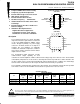
CT
RT
ERROR 1IN+
AMPLIFIER 1 1IN–
1FEEDBACK
1DTC
1OUT
GND
REF
SCP
2IN+ ERROR
2IN– AMPLIFIER 2
2FEEDBACK
2DTC
2OUT
V
CC
D, DB, N, NS, PW, OR J PACKAGE
(TOP VIEW)
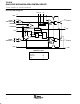
1920132
17
18
16
15
14
1312119 10
5
4
6
7
8
2IN+
2IN–
NC
2FEEDBACK
2DTC
1IN+
1IN–
NC
1FEEDBACK
IDTC
RT
CT
NC
REF
SCP
GND
NC
V
2
OUT
1OUT
FK PACKAGE
(TOP VIEW)
CC