
Datasheet

SLVS423 A− MAY 2002 − REVISED SEPTEMBER 2002
1
POST OFFICE BOX 655303 • DALLAS, TEXAS 75265
D Two Complete PWM Control Circuits
D Outputs Drive MOSFETs Directly
D Oscillator Frequency...50 kHz to 2 MHz
D 3.6-V to 20-V Supply-Voltage Range
D Low Supply Current . . . 3.5 mA Typ
D Adjustable Dead-Time Control, 0% to 100%
D 1.26-V Reference
description
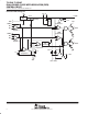
The TL1454A is a dual-channel pulse-width-mod-
ulation (PWM) control circuit, primarily intended
for low-power, dc/dc converters. Applications
include LCD displays, backlight inverters, note-
book computers, and other products requiring
small, high-frequency, dc/dc converters.
Each PWM channel has its own error amplifier, PWM comparator, dead-time control comparator, and MOSFET
driver. The voltage reference, oscillator, undervoltage lockout, and short-circuit protection are common to both
channels.
Channel 1 is configured to drive n-channel MOSFETs in step-up or flyback converters, and channel 2 is
configured to drive p-channel MOSFETs in step-down or inverting converters. The operating frequency is set
with an external resistor and an external capacitor, and dead time is continuously adjustable from 0 to 100%
duty cycle with a resistive divider network. Soft start can be implemented by adding a capacitor to the dead-time
control (DTC) network. The error-amplifier common-mode input range includes ground, which allows the
TL1454A to be used in ground-sensing battery chargers as well as voltage converters.
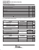
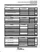
AVAILABLE OPTIONS
PACKAGED DEVICES
†
CHIP FORM
T
A
SMALL OUTLINE
(D)
PLASTIC DIP
(N)
TSSOP
(PW)
SSOP
(DB)
SOP-EIAJ
(NS)
CHIP FORM
(Y)
−20°C to 85°C TL1454ACD TL1454ACN TL1454ACPWR TL1454ACDB TL1454ACNS TL1454AY
†
The D, DB and NS packages are available taped and reeled. Add the suffix R to the device name (e.g., TL1454ACDR). The PW package is
available only left-end taped and reeled (indicated by the R suffix on the device type; e.g., TL1454ACPWR).
Copyright 2002, Texas Instruments Incorporated
! " #$%! " &$'(#! )!%*
)$#!" # ! "&%##!" &% !+% !%" %," "!$%!"
"!)) -!.* )$#! &#%""/ )%" ! %#%""(. #($)%
!%"!/ (( &%!%"*
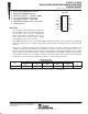
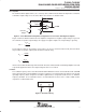
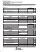
1
2
3
4
5
6
7
8
16
15
14
13
12
11
10
9
CT
RT
DTC1
IN1+
IN1−
COMP1
GND
OUT1
D, N OR PW PACKAGE
(TOP VIEW)
REF
SCP
DTC2
IN2+
IN2−
COMP2
V
CC
OUT2