TL5001EVM-097 3.3ĆV/5ĆV Selectable Output, 2.
IMPORTANT NOTICE Texas Instruments and its subsidiaries (TI) reserve the right to make changes to their products or to discontinue any product or service without notice, and advise customers to obtain the latest version of relevant information to verify, before placing orders, that information being relied on is current and complete.
Related Documentation From Texas Instruments Preface Read This First About This Manual This user’s guide is a reference manual for the TL5001EVM–097. This document provides information to assist managers and hardware engineers in application development. How to Use This Manual This manual provides the information and instructions necessary to design, construct, operate, and understand the SLVP097.
If You Need Assistance If You Need Assistance . . . If you want to . . . Contact Texas Instruments at . . . Visit TI online World Wide Web: http://www.ti.com Request more information about Texas Instruments Mixed Signal Products (MSP) World Wide Web: http://www.ti.com/sc/docs/pic/home.htm Call the Product Information Center (PIC) hotline: (972) 644–5580 Send a fax: (972) 480–7800 Write to: Texas Instruments Incorporated Product Information Center, MS 3123 P.O.
Running Title—Attribute Reference Contents 1 Hardware . . . . . . . . . . . . . . . . . . . . . . . . . . . . . . . . . . . . . . . . . . . . . . . . . . . . . . . . . . . . . . . . . . . . . . . 1.1 Introduction . . . . . . . . . . . . . . . . . . . . . . . . . . . . . . . . . . . . . . . . . . . . . . . . . . . . . . . . . . . . . . . . 1.2 Schematic . . . . . . . . . . . . . . . . . . . . . . . . . . . . . . . . . . . . . . . . . . . . . . . . . . . . . . . . . . . . . . . . . 1.
Running Title—Attribute Reference Figures 1–1 1–2 1–3 1–4 1–5 1–6 1–7 1–8 1–9 1–10 1–11 2–1 2–2 vi Typical Buck Converter Block Diagram . . . . . . . . . . . . . . . . . . . . . . . . . . . . . . . . . . . . . . . . . . . 1-2 SLVP097 Schematic . . . . . . . . . . . . . . . . . . . . . . . . . . . . . . . . . . . . . . . . . . . . . . . . . . . . . . . . . . . 1-3 I/O Connections . . . . . . . . . . . . . . . . . . . . . . . . . . . . . . . . . . . . . . . . . . . . . . . . . . . . . . . . . . . . . .
Chapter 1 Hardware The TL5001EVM–097 (SLVP097) provides a method for evaluating the performance of a buck converter using the TL5001 pulse-width-modulation (PWM) controller coupled with a TPS2817 MOSFET driver. This manual explains how to construct basic power conversion circuits including the design of the control chip functions and the basic loop. This chapter includes the following topics: Topic Page 1.1 Introduction . . . . . . . . . . . . . . . . . . . . . . . . . . . . . . . . . . . . . . . . . .
Introduction 1.1 Introduction Low cost and design simplicity make buck converters popular solutions in dc/ dc step-down applications where lack of isolation from the input source is not a concern. Loop compensation for the buck converter can be set for high bandwidths. This mode is desirable for the low peak-to-average current ratio, easing the component worst-case design parameters. Figure 1–1 shows a block diagram of a typical buck converter.
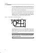
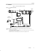
Schematic 1.2 Schematic Figure 1–2 shows the SLVP097 schematic. Figure 1–2. SLVP097 Schematic 4.5 V † to 12.6 V Input J1 1 + 2 + 3 GND 4 GND C2 0.1 µ F + C1 100 µ F 20 V CR1 30WQ04FN OUT V CC U1 TPS2817 3 2 1 RT C12 C9 0.1 µ F 1–2 = 5 V 2–3 = 3.3 V 1 2 3 R4 1.8 kΩ 7 4 3 JP1 (Optional) 8 GND SCP FB 6 C8 0.1 µ F R2 47 kΩ C6 220 µ F 10 V C10 1µ F + OUT DTC W COMP 2 V CC R8A CW 1.0 kΩ CCW C7 + 0.
Input/Output Connections 1.3 Input/Output Connections Figure 1–3 shows the SLVP097 input and output connections. Figure 1–3. I/O Connections Power Supply – + SLVP097 3.3/5 V, 2.5 AMP Rev. A.1 1997 C1 L1 + .330 C3 C8 C11 C12 U2 R4 R7 R6 R5 JP1 C13 Q1 R3 R2 C9 1.0 C10 R8 1–2 = 5 V 2–3 = 3.3 V R1 J1 IN C5 OUT + J2 1 C7 CR1 U1 1 C4 C2 + C6 – LOAD + Notes: 1) The input power supply should be rated at least 3 A with current limit set high enough for proper operation.
Board Layout 1.4 Board Layout Figures 1–4 through 1–6 show the SLVP097 board layout. Figure 1–4. Board Layout SLVP097 3.3/5V, 2.5 AMP Rev. A.1 1997 C1 L1 + .330 C3 C8 C11 C12 U2 Q1 R3 R2 C9 C10 R6 R5 OUT J2 1 + 1.0 R7 R4 C5 + C7 1.6” U1 J1 IN R1 CR1 1 C4 C2 R8 C6 1–2 = 5V 2–3 = 3.3V JP1 1 C13 2.4” Figure 1–5. Top Layer 1.6” 2.
Board Layout Figure 1–6. Bottom Layer 1.6” 2.
Bill of Material 1.5 Bill of Material Table 1–1 lists materials required for the SLVP097. Table 1–1.
Test Results 1.6 Test Results Figures 1–7 through 1–11 show test results for the the SLVP097. Figure 1–7. Output Voltage Vs Output Current (3.3-V Mode) OUTPUT VOLTAGE vs OUTPUT CURRENT (3.3-V MODE) 3.45 VCC = 9 V VO – Output Voltage – V 3.4 3.35 3.3 3.25 3.2 3.15 0 2 1 1.5 IO – Output Current – A 0.5 2.5 3 Figure 1–8. Output Voltage Vs Output Current (5-V Mode) OUTPUT VOLTAGE vs OUTPUT CURRENT (5-V MODE) 5.15 VCC = 9 V VO – Output Voltage – V 5.1 5.05 5 4.95 4.9 4.85 0 1-8 0.5 2 1 1.
Test Results Figure 1–9. Output Voltage Vs Supply Voltage (3.3-V Mode) OUTPUT VOLTAGE vs SUPPLY VOLTAGE (3.3-V MODE) 3.26 VO – Output Voltage – V 3.255 IO = 0.25 A 3.25 3.245 IO = 2.5 A 3.24 3.235 3.23 5 6 11 7 8 9 10 VCC – Supply Voltage – V 12 13 Figure 1–10. Output Voltage Vs Supply Voltage (5-V Mode) OUTPUT VOLTAGE vs SUPPLY VOLTAGE (5-V MODE) 4.92 IO = 0.25 A VO – Output Voltage – V 4.915 4.91 4.905 4.9 IO = 2.5 A 4.895 4.
Test Results Figure 1–11. Efficiency Vs Output Current (5-V Mode) EFFICIENCY vs OUTPUT CURRENT 93 92 91 5V 90 Efficiency – % 89 88 87 86 3.3 V 85 84 83 82 81 VCC = 9 V 80 0 1-10 0.5 1 1.5 IO – Output Current – A 2 2.
Chapter 2 Design Procedure The SLVP097 evaluation module provides a method for evaluating the performance of the TPS2817 MOSFET driver and the TL5001 PWM controller. The TPS2817 contains all of the circuitry necessary to drive large MOSFETs, including a voltage regulator for higher voltage applications. This section explains how to construct basic power conversion circuits including the design of the control chip functions and the basic loop. This chapter includes the following topics: Topic Page 2.
Introduction 2.1 Introduction The SLVP097 is a dc-dc buck converter module that provides a 5-V or 3.3-V output at up to 2.5 A with an input voltage range of 5.5 V to 12 V. The controller is a TL5001 PWM operating at a nominal frequency of 275 kHz. The TL5001 is configured for a maximum duty cycle of 100 percent and has short-circuit protection built in. Output voltage selection is implemented with jumper JP1.
Operating Specifications 2.2 Operating Specifications Table 2–1 lists the operating specifications for the SLVP097. Table 2–1. Operating Specifications Specification Min Input Voltage Range 4.5† Typ Max Units 12.6 V Output Voltage Range 5-V Mode 4.7 5.0 5.3 V 3.3-V Mode 3.1 3.3 3.5 V 2.6 A Output Current Range 0 Operating Frequency 275 Output Ripple Efficiency kHz 50 85% mV 90% † For 3.3 V only, minimum input voltage for 5 V output is 5.5 V.
Design Procedures 2.3 Design Procedures Detailed steps in the design of a buck-mode converter may be found in Designing With the TL5001C PWM Controller (literature number SLVA034) from Texas Instruments. This section shows the basic steps involved in this design, using the 3.3-V output mode. 2.3.1 Duty Cycle Estimate The duty cycle for a continuous-mode step-down converter is approximately: + VVO*)V Vd D I SAT Assuming the commutating diode forward voltage Vd = 0.
Design Procedures Assuming total switching time, tr+f, = 100 ns, a 55°C maximum ambient temperature, and rDS(ON) adjustment factor (for high temperature) = 1.6, then: P D + ) ƪ ƪ 2.5 2 (0.04 0.5 5.5 ǒ ƫ 1.6) 2.5 0.7 0.1 10 Ǔ ǒ *6 275 Ǔƫ + 10 3 0.41 W The thermal impedance RθJA = 90°C/W for FR-4 with 2-oz. copper and a oneinch-square pattern, thus: T 2.3.4 J + TA ) ǒq R JA P Ǔ+ D 55 ) (90 0.
Design Procedures Soft-start is added to reduce power-up transients. This is implemented by adding a capacitor across the dead-time resistor. In this design, a soft-start time of 5 ms is used: C s + 0.1 mF + RtR + 0.005 47 kW DT The TL5001 has short circuit protection (SCP) instead of a current sense circuit. If not used, the SCP terminal must be connected to ground to allow the converter to start up.
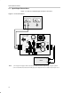
Design Procedures This information is enough to calculate the required compensation values. Figure 2–1 shows the power stage gain and phase plots. Figure 2–1. Power Stage Response 50 0 40 –45 30 –90 20 –135 10 –180 0 –225 –10 –270 –20 –315 –30 10 102 103 Frequency – Hz 104 Phase – Degrees (Dashed) Gain – dB (Solid) FREQUENCY RESPONSE –360 105 Figure 2–2 shows the required error amplifier compensation response. Figure 2–2.
Design Procedures The sum of the gains of the modulator, the LC filter, and the error amplifier needs to be 0 dB at the selected unity-gain frequency of 20 kHz. The modulator and LC filter gain is –14 dB. The two zeroes at 1.87 kHz in the compensation network that cancels the LC poles will have a total gain of 41.2 dB at 20 kHz. Therefore, the pole at zero frequency needs to furnish 0–(–14+41.2) = –27.2 dB (voltage gain = 0.04365) at 20 kHz. R5 and C12 provide this pole. R6 is already chosen as 4 kW.