
Datasheet


SLOS019E − SEPTEMBER 1988 − REVISED FEBRUARY 2005
1
POST OFFICE BOX 655303 • DALLAS, TEXAS 75265
D Extremely Low Offset Voltage ...1 µV Max
D Extremely Low Change on Offset Voltage
With Temperature . . . 0.003 µV/°C Typ
D Low Input Offset Current
500 pA Max at T
A
= − 55°C to 125°C
D A
VD
. . . 135 dB Min
D CMRR . . . 120 dB Min
D k
SVR
...110 dB Min
D Single-Supply Operation
D Common-Mode Input Voltage Range
Includes the Negative Rail
D No Noise Degradation With External
Capacitors Connected to V
DD−
description
The TLC2652 and TLC2652A are high-precision
chopper-stabilized operational amplifiers using
Texas Instruments Advanced LinCMOS pro-
cess. This process, in conjunction with unique
chopper-stabilization circuitry, produces opera-
tional amplifiers whose performance matches or
exceeds that of similar devices available today.
Chopper-stabilization techniques make possible
extremely high dc precision by continuously
nulling input offset voltage even during variations
in temperature, time, common-mode voltage, and
power supply voltage. In addition, low-frequency
noise voltage is significantly reduced. This high
precision, coupled with the extremely high input
impedance of the CMOS input stage, makes the
TLC2652 and TLC2652A an ideal choice for
low-level signal processing applications such as
strain gauges, thermocouples, and other
transducer amplifiers. For applications that
require extremely low noise and higher usable
bandwidth, use the TLC2654 or TLC2654A
device, which has a chopping frequency of
10 kHz.
The TLC2652 and TLC2652A input common-mode range includes the negative rail, thereby providing superior
performance in either single-supply or split-supply applications, even at power supply voltage levels as low as
±1.9 V.
Two external capacitors are required for operation of the device; however, the on-chip chopper-control circuitry
is transparent to the user. On devices in the 14-pin and 20-pin packages, the control circuitry is made accessible
to allow the user the option of controlling the clock frequency with an external frequency source. In addition, the
clock threshold level of the TLC2652 and TLC2652A requires no level shifting when used in the single-supply
configuration with a normal CMOS or TTL clock input.
Copyright 1988−2005, Texas Instruments Incorporated
!"#$%" & '##% & "! (')*%" %+
#"'%& "!"#$ %" &(!%"& (# %, %#$& "! -& &%#'$%&
&%# .##%/+ #"'%" (#"&&0 "& "% &&#*/ *'
%&%0 "! ** (#$%#&+
Please be aware that an important notice concerning availability, standard warranty, and use in critical applications of
Texas Instruments semiconductor products and disclaimers thereto appears at the end of this data sheet.
Advanced LinCMOS is a trademark of Texas Instruments.
1
2
3
4
8
7
6
5
C
XB
V
DD+
OUT
CLAMP
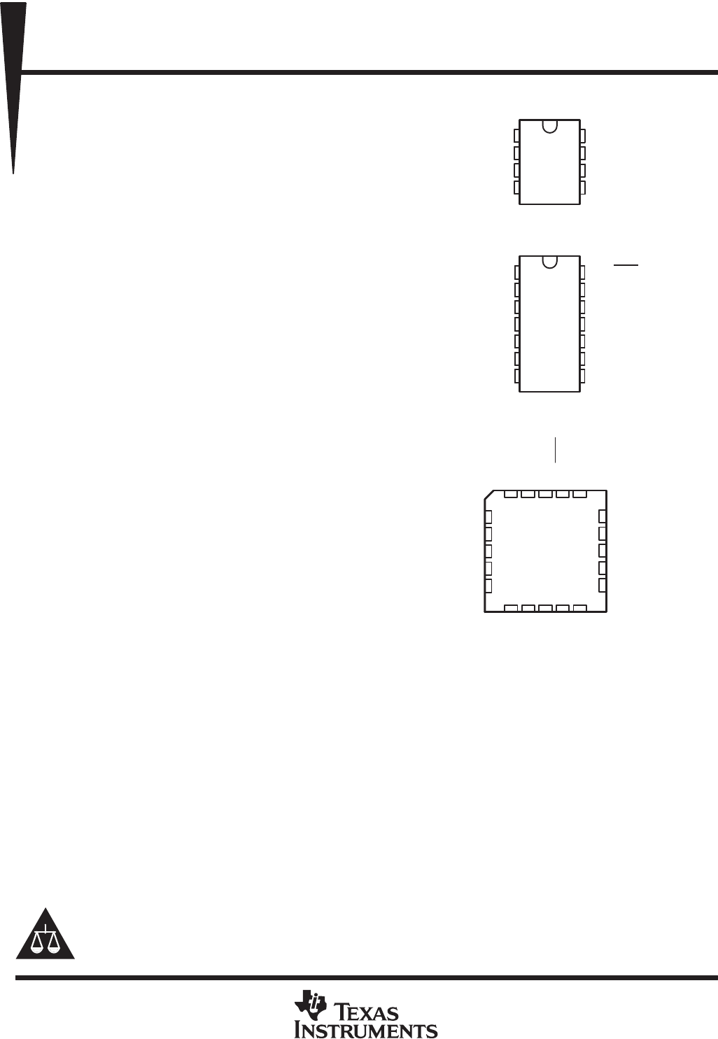
D008, JG, OR P PACKAGE
NC − No internal connection
1
2
3
4
5
6
7
14
13
12
11
10
9
8
INT/EXT
CLK IN
CLK OUT
V
DD+
OUT
CLAMP
C RETURN
D014, J, OR N PACKAGE
(TOP VIEW)
3212019
910111213
4
5
6
7
8
18
17
16
15
14
CLK OUT
NC
V
DD+
NC
OUT
FK PACKAGE
(TOP VIEW)
INT/EXT
NC
CLAMP
CLK IN
NC
NC
XA
V
C RETURN
XB
V
DD−
V
(TOP VIEW)
NC
NC
IN−
NC
IN+
C
XB
C
XA
NC
IN−
IN+
NC
V
DD−
C
XA
IN−
IN+
V
DD−
(#"'%& "$(*% %" 121 ** (#$%#& # %&%
'*&& "%,#.& "%+ ** "%,# (#"'%& (#"'%"
(#"&&0 "& "% &&#*/ *' %&%0 "! ** (#$%#&+