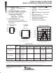
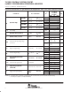
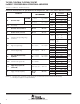
SLOS051E − OCTOBER 1987 − REVISED AUGUST 2008 D Trimmed Offset Voltage: D D D D, JG, P OR PW PACKAGE (TOP VIEW) 8 2 7 3 6 4 5 D D D D DISTRIBUTION OF TLC27M7 INPUT OFFSET VOLTAGE FK PACKAGE (TOP VIEW) VCC 2OUT 2IN − 2IN + NC 1IN − NC 1IN + NC 4 3 2 1 20 19 18 5 17 6 16 7 15 8 14 9 10 11 12 13 ÎÎÎÎÎÎÎÎÎÎÎ ÎÎÎÎÎÎÎÎÎÎÎ 30 NC 1OUT NC VDD NC 1 D NC 2OUT NC 2IN − NC 25 340 Units Tested From 2 Wafer Lo
SLOS051E − OCTOBER 1987 − REVISED AUGUST 2008 description The TLC27M2 and TLC27M7 dual operational amplifiers combine a wide range of input offset voltage grades with low offset voltage drift, high input impedance, low noise, and speeds approaching that of general-purpose bipolar devices.
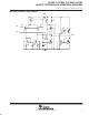
SLOS051E − OCTOBER 1987 − REVISED AUGUST 2008 equivalent schematic (each amplifier) VDD P3 P4 R6 R1 R2 IN − N5 P5 P1 P6 P2 IN + C1 R5 OUT N3 N1 R3 N2 D1 N4 R4 D2 N6 R7 N7 GND POST OFFICE BOX 655303 • DALLAS, TEXAS 75265 3
SLOS051E − OCTOBER 1987 − REVISED AUGUST 2008 absolute maximum ratings over operating free-air temperature range (unless otherwise noted)† Supply voltage, VDD (see Note 1) . . . . . . . . . . . . . . . . . . . . . . . . . . . . . . . . . . . . . . . . . . . . . . . . . . . . . . . . . . . . 18 V Differential input voltage, VID (see Note 2) . . . . . . . . . . . . . . . . . . . . . . . . . . . . . . . . . . . . . . . . . . . . .
SLOS051E − OCTOBER 1987 − REVISED AUGUST 2008 electrical characteristics at specified free-air temperature, VDD = 5 V (unless otherwise noted) PARAMETER TEST CONDITIONS TA† TLC27M2C TLC27M2AC TLC27M2BC TLC27M7C MIN VIO TLC27M2C VO = 1.4 V, RS = 50 Ω, VIC = 0, RI = 100 kΩ TLC27M2AC VO = 1.4 V, RS = 50 Ω, VIC = 0, RI = 100 kΩ Input offset voltage TLC27M2BC VO = 1.
SLOS051E − OCTOBER 1987 − REVISED AUGUST 2008 electrical characteristics at specified free-air temperature, VDD = 10 V (unless otherwise noted) PARAMETER TEST CONDITIONS TA† TLC27M2C TLC27M2AC TLC27M2BC TLC27M7C MIN VIO TLC27M2C VO = 1.4 V, RS = 50 Ω, VIC = 0, RL = 100 kΩ TLC27M2AC VO = 1.4 V, RS = 50 Ω, VIC = 0, RL = 100 kΩ Input offset voltage TLC27M2BC VO = 1.
SLOS051E − OCTOBER 1987 − REVISED AUGUST 2008 electrical characteristics at specified free-air temperature, VDD = 5 V (unless otherwise noted) PARAMETER TEST CONDITIONS TA† TLC27M2I TLC27M2AI TLC27M2BI TLC27M7I MIN VIO TLC27M2I VO = 1.4 V, RS = 50 Ω, VIC = 0, RL = 100 kΩ TLC27M2AI VO = 1.4 V, RS = 50 Ω, VIC = 0, RL = 100 kΩ Input offset voltage TLC27M2BI VO = 1.
SLOS051E − OCTOBER 1987 − REVISED AUGUST 2008 electrical characteristics at specified free-air temperature, VDD = 10 V (unless otherwise noted) PARAMETER TEST CONDITIONS TA† TLC27M2I TLC27M2AI TLC27M2BI TLC27M7I MIN VIO TLC27M2I VO = 1.4 V, RS = 50 Ω, VIC = 0, RL = 100 kΩ TLC27M2AI VO = 1.4 V, RS = 50 Ω, VIC = 0, RL = 100 kΩ Input offset voltage TLC27M2BI VO = 1.
SLOS051E − OCTOBER 1987 − REVISED AUGUST 2008 electrical characteristics at specified free-air temperature, VDD = 5 V (unless otherwise noted) PARAMETER TEST CONDITIONS TA† TLC27M2M TLC27M7M MIN VIO TLC27M2M VO = 1.4 V, RS = 50 Ω, VIC = 0, RL = 100 kΩ TLC27M7M VO = 1.
SLOS051E − OCTOBER 1987 − REVISED AUGUST 2008 electrical characteristics at specified free-air temperature, VDD = 10 V (unless otherwise noted) PARAMETER TEST CONDITIONS TA† TLC27M2M TLC27M7M MIN TLC27M2M VIO Input offset voltage TLC27M7M VO = 1.4 V, RS = 50 Ω, VIC = 0, RL = 100 kΩ VO = 1.4 V, RS = 50 Ω, VIC = 0, RL = 100 kΩ 25°C UNIT TYP MAX 1.
SLOS051E − OCTOBER 1987 − REVISED AUGUST 2008 operating characteristics at specified free-air temperature, VDD = 5 V PARAMETER TEST CONDITIONS TA TLC27M2C TLC27M2AC TLC27M2BC TLC27M7C MIN VI(PP) = 1 V SR Slew rate at unity gain RL = 100 kΩ, k , CL = 20 pF, See Figure 1 VI(PP) = 2.
SLOS051E − OCTOBER 1987 − REVISED AUGUST 2008 operating characteristics at specified free-air temperature, VDD = 5 V PARAMETER TEST CONDITIONS TA TLC27M2I TLC27M2AI TLC27M2BI TLC27M7I MIN VI(PP) = 1 V SR Slew rate at unity gain RL = 100 kΩ, k , CL = 20 pF, See Figure 1 VI(PP) = 2.
SLOS051E − OCTOBER 1987 − REVISED AUGUST 2008 operating characteristics at specified free-air temperature, VDD = 5 V PARAMETER TEST CONDITIONS TA TLC27M2M TLC27M7M MIN VI(PP) = 1 V SR Slew rate at unity gain k , RL = 100 kΩ, CL = 20 pF, See Figure 1 VI(PP) = 2.
SLOS051E − OCTOBER 1987 − REVISED AUGUST 2008 PARAMETER MEASUREMENT INFORMATION single-supply versus split-supply test circuits Because the TLC27M2 and TLC27M7 are optimized for single-supply operation, circuit configurations used for the various tests often present some inconvenience since the input signal, in many cases, must be offset from ground.
SLOS051E − OCTOBER 1987 − REVISED AUGUST 2008 PARAMETER MEASUREMENT INFORMATION input bias current Because of the high input impedance of the TLC27M2 and TLC27M7 operational amplifiers, attempts to measure the input bias current can result in erroneous readings. The bias current at normal room ambient temperature is typically less than 1 pA, a value that is easily exceeded by leakages on the test socket.
SLOS051E − OCTOBER 1987 − REVISED AUGUST 2008 PARAMETER MEASUREMENT INFORMATION input offset voltage temperature coefficient Erroneous readings often result from attempts to measure temperature coefficient of input offset voltage. This parameter is actually a calculation using input offset voltage measurements obtained at two different temperatures.
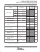
SLOS051E − OCTOBER 1987 − REVISED AUGUST 2008 TYPICAL CHARACTERISTICS Table of Graphs FIGURE VIO αVIO Input offset voltage Distribution 6, 7 Temperature coefficient Distribution 8, 9 VOH High-level output voltage vs High-level output current vs Supply voltage vs Free-air temperature 10, 11 12 13 VOL Low-level output voltage vs Common-mode input voltage vs Differential input voltage vs Free-air temperature vs Low-l
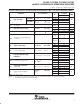
SLOS051E − OCTOBER 1987 − REVISED AUGUST 2008 TYPICAL CHARACTERISTICS DISTRIBUTION OF TLC27M2 INPUT OFFSET VOLTAGE DISTRIBUTION OF TLC27M2 INPUT OFFSET VOLTAGE ÎÎÎÎÎÎÎÎÎÎÎÎ ÎÎÎÎÎÎÎÎÎÎÎÎ 60 50 Percentage of Units − % 50 Percentage of Units − % 60 612 Amplifiers Tested From 4 Wafer Lots VDD = 5 V TA = 25°C P Package 40 30 20 10 ÎÎÎÎÎÎÎÎÎÎÎ ÎÎÎÎÎÎÎÎÎÎÎ 612 Amplifiers Tested From 4 Wafer Lots VDD = 10 V TA = 25°C P Pack
SLOS051E − OCTOBER 1987 − REVISED AUGUST 2008 TYPICAL CHARACTERISTICS† HIGH-LEVEL OUTPUT VOLTAGE vs HIGH-LEVEL OUTPUT CURRENT HIGH-LEVEL OUTPUT VOLTAGE vs HIGH-LEVEL OUTPUT CURRENT 5 VOH − High-Level Output Voltage − V VOH VOH − High-Level Output Voltage − V VOH 4 ÎÎÎÎ ÎÎÎÎÎÎÎÎ ÎÎÎÎ VDD = 5 V 3 VDD = 4 V ÁÁ ÁÁ ÁÁ ÁÁÁÁÁ ÁÁÁÁÁ ÎÎÎÎÎÎ ÎÎÎÎÎÎ 16 VID = 100 mV TA = 25°C VDD = 3 V 2 ÁÁ ÁÁ ÁÁ 1 0 0 −2 −4 −6 −8 IOH − H
SLOS051E − OCTOBER 1987 − REVISED AUGUST 2008 TYPICAL CHARACTERISTICS† LOW-LEVEL OUTPUT VOLTAGE vs COMMON-MODE INPUT VOLTAGE LOW-LEVEL OUTPUT VOLTAGE vs COMMON-MODE INPUT VOLTAGE ÁÁ ÁÁ 500 VDD = 5 V IOL = 5 mA TA = 25°C 650 VOL VOL − Low-Level Output Voltage − mV VOL VOL − Low-Level Output Voltage − mV 700 600 550 VID = − 100 mV 500 450 450 400 VID = − 100 mV VID = − 1 V 350 VID = − 2.
SLOS051E − OCTOBER 1987 − REVISED AUGUST 2008 TYPICAL CHARACTERISTICS† LOW-LEVEL OUTPUT VOLTAGE vs LOW-LEVEL OUTPUT CURRENT LOW-LEVEL OUTPUT VOLTAGE vs LOW-LEVEL OUTPUT CURRENT ÁÁÁÁÁ ÁÁÁÁÁ ÁÁÁÁÁ ÁÁÁÁÁ 3 1 VOL − Low-Level Output Voltage − V VOL 0.9 ÁÁ ÁÁ ÁÁ 0.8 VOL − Low-Level Output Voltage − V VOL VID = − 1 V VIC = 0.5 V TA = 25°C VDD = 5 V 0.7 0.6 VDD = 4 V VDD = 3 V 0.5 0.4 0.2 0.
SLOS051E − OCTOBER 1987 − REVISED AUGUST 2008 TYPICAL CHARACTERISTICS† COMMON-MODE INPUT VOLTAGE POSITIVE LIMIT vs SUPPLY VOLTAGE 16 10000 TA = 25°C VDD = 10 V VIC = 5 V See Note A ÎÎ ÎÎ 1000 IIB 100 VIC − Common-Mode Input Voltage − V VIC IIB I IO − input Bias and Offset Currents − pA I IB and IIO INPUT BIAS CURRENT AND INPUT OFFSET CURRENT vs FREE-AIR TEMPERATURE ÎÎ ÎÎ IIO 10 12 10 8 ÁÁ ÁÁ ÁÁ 1 0.
SLOS051E − OCTOBER 1987 − REVISED AUGUST 2008 TYPICAL CHARACTERISTICS† SLEW RATE vs SUPPLY VOLTAGE 0.9 ÎÎÎÎÎ 0.6 0.5 0.4 0.3 2 4 6 8 10 12 VDD − Supply Voltage − V 14 0.5 ÁÁÁÁÁ ÁÁÁÁÁÁÁÁÁÁ ÁÁÁÁÁ VDD = 5 V VI(PP) = 1 V 0.2 − 75 − 50 16 MAXIMUM PEAK-TO-PEAK OUTPUT VOLTAGE vs FREQUENCY VO(PP) − Maximum Peak-to-Peak Output Voltage − V 1.4 Normalized Slew Rate 1.2 1.
SLOS051E − OCTOBER 1987 − REVISED AUGUST 2008 TYPICAL CHARACTERISTICS† UNITY-GAIN BANDWIDTH vs FREE-AIR TEMPERATURE ÁÁÁÁÁ ÁÁÁÁÁ ÁÁÁÁÁ ÁÁÁÁÁ 900 800 VDD = 5 V VI = 10 mV CL = 20 pF See Figure 3 800 700 750 B1 B1 − Unity-Gain Bandwidth − kHz B1 B1 − Unity-Gain Bandwidth − kHz UNITY-GAIN BANDWIDTH vs SUPPLY VOLTAGE 600 500 400 700 ÁÁÁÁÁ ÁÁÁÁÁ ÁÁÁÁÁ ÁÁÁÁÁ VI = 10 mV CL = 20 pF TA = 25°C See Figure 3 650 600 550 500 4
SLOS051E − OCTOBER 1987 − REVISED AUGUST 2008 TYPICAL CHARACTERISTICS† LARGE-SCALE DIFFERENTIAL VOLTAGE AMPLIFICATION AND PHASE SHIFT vs FREQUENCY 10 7 VDD = 10 V RL = 100 kΩ TA = 25°C ÁÁ ÁÁ ÁÁ 10 5 0° ÎÎÎ ÎÎÎ 10 4 30° AVD 10 3 60° 10 2 90° Phase Shift AVD AVD − Large-Signal Differential Voltage Amplification 10 6 Phase Shift 10 120° 1 150° 0.
SLOS051E − OCTOBER 1987 − REVISED AUGUST 2008 TYPICAL CHARACTERISTICS PHASE MARGIN vs CAPACITIVE LOAD 44° VDD = 5 V VI = 10 mV TA = 25°C See Figure 3 42° φm m − Phase Margin 40° ÁÁ ÁÁ 38° 36° 34° 32° 30° 28° 0 10 20 30 40 50 60 70 80 CL − Capacitive Load − pF 90 100 Figure 36 nV/ Hz Vn V n− Equivalent Input Noise Voltage − nV/Hz ÁÁ ÁÁ ÁÁ EQUIVALENT INPUT NOISE VOLTAGE vs FREQUENCY 300 VDD = 5 V RS = 20 Ω TA = 25°C
SLOS051E − OCTOBER 1987 − REVISED AUGUST 2008 APPLICATION INFORMATION single-supply operation While the TLC27M2 and TLC27M7 perform well using dual power supplies (also called balanced or split supplies), the design is optimized for single-supply operation. This design includes an input common-mode voltage range that encompasses ground, as well as an output voltage range that pulls down to ground.
SLOS051E − OCTOBER 1987 − REVISED AUGUST 2008 APPLICATION INFORMATION input characteristics The TLC27M2 and TLC27M7 are specified with a minimum and a maximum input voltage that, if exceeded at either input, could cause the device to malfunction. Exceeding this specified range is a common problem, especially in single-supply operation.
SLOS051E − OCTOBER 1987 − REVISED AUGUST 2008 APPLICATION INFORMATION (a) CL = 20 pF, RL = NO LOAD (b) CL = 170 pF, RL = NO LOAD 2.5 V − VO + VI CL TA = 25°C f = 1 kHz VI(PP) = 1 V −2.5 V (c) CL = 190 pF, RL = NO LOAD (d) TEST CIRCUIT Figure 41.
SLOS051E − OCTOBER 1987 − REVISED AUGUST 2008 APPLICATION INFORMATION output characteristics (continued) VDD VI + RP IP VO − C IP R2 IL R1 RL − P + V I F DD ) I VO *V L O ) I + R P IP = Pullup current required by the operational amplifier (typically 500 µA) Figure 42. Resistive Pullup to Increase VOH Figure 43.
SLOS051E − OCTOBER 1987 − REVISED AUGUST 2008 APPLICATION INFORMATION 1N4148 470 kΩ 100 kΩ 5V 1/2 TLC27M2 5V − 47 kΩ 100 kΩ VI VO + IS 1/2 TLC27M7 + − 2N3821 R2 68 kΩ 100 kΩ 1 µF R1 68 kΩ C2 2.2 nF C1 2.2 nF R NOTES: VO(PP) ≈ 2 V f O + NOTES: VI = 0 V to 3 V V I + I S R 1 2p ǸR1R2C1C2 Figure 45. Precision Low-Current Sink Figure 44.
SLOS051E − OCTOBER 1987 − REVISED AUGUST 2008 APPLICATION INFORMATION 10 MΩ VDD − 1 kΩ − 1/2 TLC27M2 VO 1/2 TLC27M2 VREF + 15 nF + 100 kΩ 150 pF NOTES: VDD = 4 V to 15 V Vref = 0 V to VDD − 2 V Figure 47. Photo-Diode Amplifier With Ambient Light Rejection 1 MΩ VDD 33 pF − VO + 1/2 TLC27M2 1N4148 100 kΩ 100 kΩ NOTES: VDD = 8 V to 16 V VO = 5 V, 10 mA Figure 48.
SLOS051E − OCTOBER 1987 − REVISED AUGUST 2008 APPLICATION INFORMATION 5V 0.1 µ F VI 1 MΩ 0.22 µF + VO − 1/2 TLC27M2 1 MΩ 100 kΩ 100 kΩ 10 kΩ 0.1 µF Figure 49.
PACKAGE OPTION ADDENDUM www.ti.
PACKAGE OPTION ADDENDUM www.ti.
PACKAGE OPTION ADDENDUM www.ti.
PACKAGE OPTION ADDENDUM www.ti.
PACKAGE OPTION ADDENDUM www.ti.com 11-Apr-2013 (2) Eco Plan - The planned eco-friendly classification: Pb-Free (RoHS), Pb-Free (RoHS Exempt), or Green (RoHS & no Sb/Br) - please check http://www.ti.com/productcontent for the latest availability information and additional product content details. TBD: The Pb-Free/Green conversion plan has not been defined.
PACKAGE MATERIALS INFORMATION www.ti.com 8-Jul-2013 TAPE AND REEL INFORMATION *All dimensions are nominal Device Package Package Pins Type Drawing SPQ Reel Reel A0 Diameter Width (mm) (mm) W1 (mm) B0 (mm) K0 (mm) P1 (mm) W Pin1 (mm) Quadrant TLC27M2ACDR SOIC D 8 2500 330.0 12.4 6.4 5.2 2.1 8.0 12.0 Q1 TLC27M2AIDR SOIC D 8 2500 330.0 12.4 6.4 5.2 2.1 8.0 12.0 Q1 TLC27M2BCDR SOIC D 8 2500 330.0 12.4 6.4 5.2 2.1 8.0 12.0 Q1 TLC27M2BIDR SOIC D 8 2500 330.
PACKAGE MATERIALS INFORMATION www.ti.com 8-Jul-2013 *All dimensions are nominal Device Package Type Package Drawing Pins SPQ Length (mm) Width (mm) Height (mm) TLC27M2ACDR SOIC D 8 2500 340.5 338.1 20.6 TLC27M2AIDR SOIC D 8 2500 340.5 338.1 20.6 TLC27M2BCDR SOIC D 8 2500 340.5 338.1 20.6 TLC27M2BIDR SOIC D 8 2500 340.5 338.1 20.6 TLC27M2CDR SOIC D 8 2500 340.5 338.1 20.6 TLC27M2CPSR SO PS 8 2000 367.0 367.0 38.0 TLC27M2CPWR TSSOP PW 8 2000 367.
MECHANICAL DATA MCER001A – JANUARY 1995 – REVISED JANUARY 1997 JG (R-GDIP-T8) CERAMIC DUAL-IN-LINE 0.400 (10,16) 0.355 (9,00) 8 5 0.280 (7,11) 0.245 (6,22) 1 0.063 (1,60) 0.015 (0,38) 4 0.065 (1,65) 0.045 (1,14) 0.310 (7,87) 0.290 (7,37) 0.020 (0,51) MIN 0.200 (5,08) MAX Seating Plane 0.130 (3,30) MIN 0.023 (0,58) 0.015 (0,38) 0°–15° 0.100 (2,54) 0.014 (0,36) 0.008 (0,20) 4040107/C 08/96 NOTES: A. B. C. D. E. All linear dimensions are in inches (millimeters).
IMPORTANT NOTICE Texas Instruments Incorporated and its subsidiaries (TI) reserve the right to make corrections, enhancements, improvements and other changes to its semiconductor products and services per JESD46, latest issue, and to discontinue any product or service per JESD48, latest issue. Buyers should obtain the latest relevant information before placing orders and should verify that such information is current and complete.