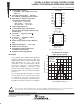
TLC27M4, TLC27M4A, TLC27M4B, TLC27M4Y, TLC27M9 LinCMOS PRECISION QUAD OPERATIONAL AMPLIFIERS SLOS093C – OCTOBER 1987 – REVISED MAY 1999 D D D D D D D D D D 1OUT 1IN – 1IN + VDD 2IN + 2IN – 2OUT 1 14 2 13 3 12 4 11 5 10 6 9 7 8 4OUT 4IN – 4IN + GND 3IN + 3IN – 3OUT FK PACKAGE (TOP VIEW) 1IN – 1OUT NC 4OUT 4IN – D D, J, N, OR PW PACKAGE (TOP VIEW) Trimmed Offset Voltage: TLC27M9 . . . 900 µV Max at TA = 25°C, VDD = 5 V Input Offset Voltage Drift . . . Typically 0.
TLC27M4, TLC27M4A, TLC27M4B, TLC27M4Y, TLC27M9 LinCMOS PRECISION QUAD OPERATIONAL AMPLIFIERS SLOS093C – OCTOBER 1987 – REVISED MAY 1999 description (continued) Four offset voltage grades are available (C-suffix and I-suffix types), ranging from the low-cost TLC27M4 (10 mV) to the high-precision TLC27M9 (900 µV).
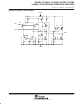
TLC27M4, TLC27M4A, TLC27M4B, TLC27M4Y, TLC27M9 LinCMOS PRECISION QUAD OPERATIONAL AMPLIFIERS SLOS093C – OCTOBER 1987 – REVISED MAY 1999 equivalent schematic (each amplifier) VDD P3 P4 R6 R1 R2 IN – N5 P5 P1 P6 P2 IN + C1 R5 OUT N3 N1 R3 N2 D1 N4 R4 D2 N6 N7 R7 GND POST OFFICE BOX 655303 • DALLAS, TEXAS 75265 3
TLC27M4, TLC27M4A, TLC27M4B, TLC27M4Y, TLC27M9 LinCMOS PRECISION QUAD OPERATIONAL AMPLIFIERS SLOS093C – OCTOBER 1987 – REVISED MAY 1999 TLC27M4Y chip information This chip, when properly assembled, displays characteristics similar to the TLC27M4C. Thermal compression or ultrasonic bonding may be used on the doped-aluminum bonding pads. Chips may be mounted with conductive epoxy or a gold-silicon preform.
TLC27M4, TLC27M4A, TLC27M4B, TLC27M4Y, TLC27M9 LinCMOS PRECISION QUAD OPERATIONAL AMPLIFIERS SLOS093C – OCTOBER 1987 – REVISED MAY 1999 absolute maximum ratings over operating free-air temperature range (unless otherwise noted)† Supply voltage, VDD (see Note 1) . . . . . . . . . . . . . . . . . . . . . . . . . . . . . . . . . . . . . . . . . . . . . . . . . . . . . . . . . . . . 18 V Differential input voltage, VID (see Note 2) . . . . . . . . . . . . . . . . . . . . . . . . . . . . . . . . . . . . . . .
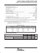
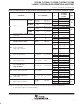
TLC27M4, TLC27M4A, TLC27M4B, TLC27M4Y, TLC27M9 LinCMOS PRECISION QUAD OPERATIONAL AMPLIFIERS SLOS093C – OCTOBER 1987 – REVISED MAY 1999 electrical characteristics at specified free-air temperature, VDD = 5 V (unless otherwise noted) PARAMETER TEST CONDITIONS TA† TLC27M4C TLC27M4AC TLC27M4BC TLC27M9C MIN VIO TLC27M4C VO = 1.4 V,, RS = 50 Ω, VIC = 0,, RL = 100 kΩ TLC27M4AC VO = 1.4 V,, RS = 50 Ω, VIC = 0,, RL = 100 kΩ Full range TLC274BC VO = 1.
TLC27M4, TLC27M4A, TLC27M4B, TLC27M4Y, TLC27M9 LinCMOS PRECISION QUAD OPERATIONAL AMPLIFIERS SLOS093C – OCTOBER 1987 – REVISED MAY 1999 electrical characteristics at specified free-air temperature, VDD = 10 V (unless otherwise noted) PARAMETER TEST CONDITIONS TA† TLC27M4C TLC27M4AC TLC27M4BC TLC27M9C MIN VIO TLC27M4C VO = 1.4 V,, RS = 50 Ω, VIC = 0,, RL = 100 kΩ TLC27M4AC VO = 1.4 V,, RS = 50 Ω, VIC = 0,, RL = 100 kΩ Full range TLC27M4BC VO = 1.
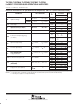
TLC27M4, TLC27M4A, TLC27M4B, TLC27M4Y, TLC27M9 LinCMOS PRECISION QUAD OPERATIONAL AMPLIFIERS SLOS093C – OCTOBER 1987 – REVISED MAY 1999 electrical characteristics at specified free-air temperature, VDD = 5 V (unless otherwise noted) PARAMETER TEST CONDITIONS TA† TLC27M4I TLC27M4AI TLC27M4BI TLC27M9I MIN VIO TLC27M4I VO = 1.4 V,, RS = 50 Ω, VIC = 0,, RL = 100 kΩ TLC27M4AI VO = 1.4 V,, RS = 50 Ω, VIC = 0,, RL = 100 kΩ Full range TLC27M4BI VO = 1.
TLC27M4, TLC27M4A, TLC27M4B, TLC27M4Y, TLC27M9 LinCMOS PRECISION QUAD OPERATIONAL AMPLIFIERS SLOS093C – OCTOBER 1987 – REVISED MAY 1999 electrical characteristics at specified free-air temperature, VDD = 10 V (unless otherwise noted) PARAMETER TEST CONDITIONS TA† TLC27M4I TLC27M4AI TLC27M4BI TLC27M9I MIN VIO 25°C TLC27M4I VO = 1.4 V,, RS = 50 Ω, VIC = 0,, RL = 100 kΩ TLC27M4AI VO = 1.4 V,, RS = 50 Ω, VIC = 0,, RL = 100 kΩ Full range TLC27M4BI VO = 1.
TLC27M4, TLC27M4A, TLC27M4B, TLC27M4Y, TLC27M9 LinCMOS PRECISION QUAD OPERATIONAL AMPLIFIERS SLOS093C – OCTOBER 1987 – REVISED MAY 1999 electrical characteristics at specified free-air temperature, VDD = 5 V (unless otherwise noted) PARAMETER TEST CONDITIONS TA† TLC27M4M TLC27M9M MIN VIO TLC27M4M VO = 1.4 V,, RS = 50 Ω, VIC = 0,, RL = 100 kΩ TLC27M9M VO = 1.
TLC27M4, TLC27M4A, TLC27M4B, TLC27M4Y, TLC27M9 LinCMOS PRECISION QUAD OPERATIONAL AMPLIFIERS SLOS093C – OCTOBER 1987 – REVISED MAY 1999 electrical characteristics at specified free-air temperature, VDD = 10 V (unless otherwise noted) PARAMETER TEST CONDITIONS TA† TLC27M4M TLC27M9M MIN VIO VO = 1.4 V,, RS = 50 Ω, VIC = 0,, RL = 100 kΩ Full range TLC27M9M VO = 1.
TLC27M4, TLC27M4A, TLC27M4B, TLC27M4Y, TLC27M9 LinCMOS PRECISION QUAD OPERATIONAL AMPLIFIERS SLOS093C – OCTOBER 1987 – REVISED MAY 1999 electrical characteristics, VDD = 5 V, TA = 25°C (unless otherwise noted) PARAMETER TEST CONDITIONS VIO Input offset voltage VO = 1.4 V,, RS = 50 Ω, αVIO Temperature coefficient of input offset voltage TA = 25°C to 70°C IIO IIB Input offset current (see Note 4) VO = 2.5 V, VO = 2.
TLC27M4, TLC27M4A, TLC27M4B, TLC27M4Y, TLC27M9 LinCMOS PRECISION QUAD OPERATIONAL AMPLIFIERS SLOS093C – OCTOBER 1987 – REVISED MAY 1999 operating characteristics at specified free-air temperature, VDD = 5 V PARAMETER TEST CONDITIONS TA TLC27M4C TLC27M4AC TLC27M4BC TLC27M9C MIN SR Slew rate at unity gain RL = 100 Ω, CL = 20 pF pF, See Figure 1 VIPP = 1 V VIPP = 2.
TLC27M4, TLC27M4A, TLC27M4B, TLC27M4Y, TLC27M9 LinCMOS PRECISION QUAD OPERATIONAL AMPLIFIERS SLOS093C – OCTOBER 1987 – REVISED MAY 1999 operating characteristics at specified free-air temperature, VDD = 5 V PARAMETER TEST CONDITIONS TA TLC27M4I TLC27M4AI TLC27M4BI TLC27M9I MIN SR Slew rate at unity gain RL = 100 Ω, CL = 20 pF pF, See Figure 1 VIPP = 1 V VIPP = 2.
TLC27M4, TLC27M4A, TLC27M4B, TLC27M4Y, TLC27M9 LinCMOS PRECISION QUAD OPERATIONAL AMPLIFIERS SLOS093C – OCTOBER 1987 – REVISED MAY 1999 operating characteristics at specified free-air temperature, VDD = 5 V PARAMETER TEST CONDITIONS TA TLC27M4M TLC27M9M MIN SR Slew rate at unity gain RL = 100 Ω, CL = 20 pF pF, See Figure 1 VIPP = 1 V VIPP = 2.
TLC27M4, TLC27M4A, TLC27M4B, TLC27M4Y, TLC27M9 LinCMOS PRECISION QUAD OPERATIONAL AMPLIFIERS SLOS093C – OCTOBER 1987 – REVISED MAY 1999 operating characteristics, VDD = 5 V, TA = 25°C PARAMETER SR Slew rate at unity gain TEST CONDITIONS TLC27M4Y MIN TYP RL = 100 kΩ, CL = 20 pF pF, See Figure 1 VIPP = 1 V 0.43 VIPP = 2.5 V 0.
TLC27M4, TLC27M4A, TLC27M4B, TLC27M4Y, TLC27M9 LinCMOS PRECISION QUAD OPERATIONAL AMPLIFIERS SLOS093C – OCTOBER 1987 – REVISED MAY 1999 PARAMETER MEASUREMENT INFORMATION single-supply versus split-supply test circuits Because the TLC27M4 and TLC27M9 are optimized for single-supply operation, circuit configurations used for the various tests often present some inconvenience since the input signal, in many cases, must be offset from ground.
TLC27M4, TLC27M4A, TLC27M4B, TLC27M4Y, TLC27M9 LinCMOS PRECISION QUAD OPERATIONAL AMPLIFIERS SLOS093C – OCTOBER 1987 – REVISED MAY 1999 PARAMETER MEASUREMENT INFORMATION input bias current Because of the high input impedance of the TLC27M4 and TLC27M9 operational amplifiers, attempts to measure the input bias current can result in erroneous readings. The bias current at normal room ambient temperature is typically less than 1 pA, a value that is easily exceeded by leakages on the test socket.
TLC27M4, TLC27M4A, TLC27M4B, TLC27M4Y, TLC27M9 LinCMOS PRECISION QUAD OPERATIONAL AMPLIFIERS SLOS093C – OCTOBER 1987 – REVISED MAY 1999 PARAMETER MEASUREMENT INFORMATION input offset voltage temperature coefficient Erroneous readings often result from attempts to measure temperature coefficient of input offset voltage. This parameter is actually a calculation using input offset voltage measurements obtained at two different temperatures.
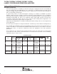
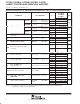
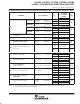
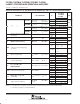
TLC27M4, TLC27M4A, TLC27M4B, TLC27M4Y, TLC27M9 LinCMOS PRECISION QUAD OPERATIONAL AMPLIFIERS SLOS093C – OCTOBER 1987 – REVISED MAY 1999 TYPICAL CHARACTERISTICS Table of Graphs FIGURE VIO αVIO Input offset voltage Distribution 6, 7 Temperature coefficient of input offset voltage Distribution 8, 9 VOH High level output voltage High-level vs High-level output current vs Supply voltage vs Free-air temperature 10, 11 12 13 VOL Low level output voltage Low-level vs Common-mode input voltage vs Diff
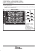
TLC27M4, TLC27M4A, TLC27M4B, TLC27M4Y, TLC27M9 LinCMOS PRECISION QUAD OPERATIONAL AMPLIFIERS SLOS093C – OCTOBER 1987 – REVISED MAY 1999 TYPICAL CHARACTERISTICS DISTRIBUTION OF TLC27M4 INPUT OFFSET VOLTAGE DISTRIBUTION OF TLC27M4 INPUT OFFSET VOLTAGE 60 60 612 Amplifiers Tested From 6 Wafer Lots VDD = 5 V TA = 25°C N Package 50 Percentage of Units – % Percentage of Units – % 50 612 Amplifiers Tested From 4 Wafer Lots VDD = 10 V TA = 25°C N Package 40 30 20 10 40 30 20 10 0 0 –5 –4 –3 –2
TLC27M4, TLC27M4A, TLC27M4B, TLC27M4Y, TLC27M9 LinCMOS PRECISION QUAD OPERATIONAL AMPLIFIERS SLOS093C – OCTOBER 1987 – REVISED MAY 1999 TYPICAL CHARACTERISTICS† HIGH-LEVEL OUTPUT VOLTAGE vs HIGH-LEVEL OUTPUT CURRENT HIGH-LEVEL OUTPUT VOLTAGE vs HIGH-LEVEL OUTPUT CURRENT 16 VID = 100 mV TA = 25°C VOH – High-Level Output Voltage – V VOH – High-Level Output Voltage – V 5 4 VDD = 5 V 3 VDD = 4 V VDD = 3 V 2 1 14 VDD = 16 V 12 10 8 VDD = 10 V 6 4 2 0 0 0 –2 –4 –6 –8 IOH – High-Level Output Current
TLC27M4, TLC27M4A, TLC27M4B, TLC27M4Y, TLC27M9 LinCMOS PRECISION QUAD OPERATIONAL AMPLIFIERS SLOS093C – OCTOBER 1987 – REVISED MAY 1999 TYPICAL CHARACTERISTICS† LOW-LEVEL OUTPUT VOLTAGE vs COMMON-MODE INPUT VOLTAGE LOW-LEVEL OUTPUT VOLTAGE vs COMMON-MODE INPUT VOLTAGE 500 VDD = 5 V IOL = 5 mA TA = 25°C 650 VOL – Low-Level Output Voltage – mV VOL – Low-Level Output Voltage – mV 700 600 550 VID = – 100 mV 500 450 400 VID = – 1 V 350 450 400 VID = – 100 mV 0.5 1.5 2.5 3.
TLC27M4, TLC27M4A, TLC27M4B, TLC27M4Y, TLC27M9 LinCMOS PRECISION QUAD OPERATIONAL AMPLIFIERS SLOS093C – OCTOBER 1987 – REVISED MAY 1999 TYPICAL CHARACTERISTICS† LOW-LEVEL OUTPUT VOLTAGE vs LOW-LEVEL OUTPUT CURRENT LOW-LEVEL OUTPUT VOLTAGE vs LOW-LEVEL OUTPUT CURRENT 1 3 VOL – Low-Level Output Voltage – V 0.9 0.8 VOL – Low-Level Output Voltage – V VID = – 1 V VIC = 0.5 V TA = 25°C VDD = 5 V 0.7 VDD = 4 V 0.6 VDD = 3 V 0.5 0.4 0.3 0.2 0.
TLC27M4, TLC27M4A, TLC27M4B, TLC27M4Y, TLC27M9 LinCMOS PRECISION QUAD OPERATIONAL AMPLIFIERS SLOS093C – OCTOBER 1987 – REVISED MAY 1999 TYPICAL CHARACTERISTICS† COMMON-MODE INPUT VOLTAGE POSITIVE LIMIT vs SUPPLY VOLTAGE 10000 16 VDD = 10 V VIC = 5 V See Note A TA = 25°C VIC – Common-Mode Input Voltage – V I IB and I IO – Input Bias and Offset Currents – pA INPUT BIAS CURRENT AND INPUT OFFSET CURRENT vs FREE-AIR TEMPERATURE 1000 IIB 100 IIO 10 1 0.
TLC27M4, TLC27M4A, TLC27M4B, TLC27M4Y, TLC27M9 LinCMOS PRECISION QUAD OPERATIONAL AMPLIFIERS SLOS093C – OCTOBER 1987 – REVISED MAY 1999 TYPICAL CHARACTERISTICS† SLEW RATE vs SUPPLY VOLTAGE 0.9 0.9 AV = 1 VIPP = 1 V RL = 100 kΩ CL = 20 pF TA = 25°C See Figure 1 0.8 SR – Slew Rate – V/ µs 0.8 SR – Slew Rate – V/ µs SLEW RATE vs FREE-AIR TEMPERATURE 0.7 0.6 0.5 0.4 VDD = 10 V VIPP = 5.5 V 0.7 0.6 VDD = 10 V VIPP = 1 V 0.5 0.4 VDD = 5 V VIPP = 1 V 0.3 0.
TLC27M4, TLC27M4A, TLC27M4B, TLC27M4Y, TLC27M9 LinCMOS PRECISION QUAD OPERATIONAL AMPLIFIERS SLOS093C – OCTOBER 1987 – REVISED MAY 1999 TYPICAL CHARACTERISTICS† UNITY-GAIN BANDWIDTH vs FREE-AIR TEMPERATURE UNITY-GAIN BANDWIDTH vs SUPPLY VOLTAGE 800 VDD = 5 V VI = 10 mV CL = 20 pF See Figure 3 800 VI = 10 mV CL = 20 pF TA = 25°C See Figure 3 750 B1 – Unity-Gain Bandwidth – kHz B1 – Unity-Gain Bandwidth – kHz 900 700 600 500 400 700 650 600 550 500 450 300 – 75 400 – 50 – 25 0 25 50 75 100 TA
TLC27M4, TLC27M4A, TLC27M4B, TLC27M4Y, TLC27M9 LinCMOS PRECISION QUAD OPERATIONAL AMPLIFIERS SLOS093C – OCTOBER 1987 – REVISED MAY 1999 TYPICAL CHARACTERISTICS† LARGE-SIGNAL DIFFERENTIAL VOLTAGE AMPLIFICATION AND PHASE SHIFT vs FREQUENCY 107 VDD = 10 V RL = 100 kΩ TA = 25°C ÁÁ ÁÁ ÁÁ ÌÌ ÌÌ 105 0° AVD 10 4 30° 103 60° 102 90° Phase Shift AVD A VD – Large-Signal Differential Voltage Amplification 106 Phase Shift 101 120° 1 150° 0.
TLC27M4, TLC27M4A, TLC27M4B, TLC27M4Y, TLC27M9 LinCMOS PRECISION QUAD OPERATIONAL AMPLIFIERS SLOS093C – OCTOBER 1987 – REVISED MAY 1999 TYPICAL CHARACTERISTICS PHASE MARGIN vs CAPACITIVE LOAD 44° VDD = 5 V VI = 10 mV TA = 25°C See Figure 3 42° φ m – Phase Margin 40° 38° 36° 34° 32° 30° 28° 0 10 20 30 40 50 60 70 80 CL – Capacitive Load – pF 90 100 Figure 36 EQUIVALENT INPUT NOISE VOLTAGE vs FREQUENCY Vn – Equivalent Input Noise Voltage – nV/ Hz 300 VDD = 5 V RS = 20 Ω TA = 25°C See Figure 2 250
TLC27M4, TLC27M4A, TLC27M4B, TLC27M4Y, TLC27M9 LinCMOS PRECISION QUAD OPERATIONAL AMPLIFIERS SLOS093C – OCTOBER 1987 – REVISED MAY 1999 APPLICATION INFORMATION single-supply operation While the TLC27M4 and TLC27M9 perform well using dual power supplies (also called balanced or split supplies), the design is optimized for single-supply operation. This design includes an input common-mode voltage range that encompasses ground as well as an output voltage range that pulls down to ground.
TLC27M4, TLC27M4A, TLC27M4B, TLC27M4Y, TLC27M9 LinCMOS PRECISION QUAD OPERATIONAL AMPLIFIERS SLOS093C – OCTOBER 1987 – REVISED MAY 1999 APPLICATION INFORMATION single-supply operation (continued) – Output Logic Logic Logic Power Supply + (a) COMMON SUPPLY RAILS – + Output Logic Logic Logic Power Supply (b) SEPARATE BYPASSED SUPPLY RAILS (preferred) Figure 39.
TLC27M4, TLC27M4A, TLC27M4B, TLC27M4Y, TLC27M9 LinCMOS PRECISION QUAD OPERATIONAL AMPLIFIERS SLOS093C – OCTOBER 1987 – REVISED MAY 1999 APPLICATION INFORMATION noise performance (continued) – – VO + + VI (b) INVERTING AMPLIFIER (a) NONINVERTING AMPLIFIER VO + – VI VI VO (c) UNITY-GAIN AMPLIFIER Figure 40. Guard-Ring Schemes output characteristics The output stage of the TLC27M4 and TLC27M9 is designed to sink and source relatively high amounts of current (see typical characteristics).
TLC27M4, TLC27M4A, TLC27M4B, TLC27M4Y, TLC27M9 LinCMOS PRECISION QUAD OPERATIONAL AMPLIFIERS SLOS093C – OCTOBER 1987 – REVISED MAY 1999 APPLICATION INFORMATION output characteristics (continued) Although the TLC27M4 and TLC27M9 possess excellent high-level output voltage and current capability, methods for boosting this capability are available, if needed. The simplest method involves the use of a pullup resistor (RP) connected from the output to the positive supply rail (see Figure 42).
TLC27M4, TLC27M4A, TLC27M4B, TLC27M4Y, TLC27M9 LinCMOS PRECISION QUAD OPERATIONAL AMPLIFIERS SLOS093C – OCTOBER 1987 – REVISED MAY 1999 APPLICATION INFORMATION latch-up (continued) The current path established if latch-up occurs is usually between the positive supply rail and ground; it can be triggered by surges on the supply lines and/or voltages on either the output or inputs that exceed the supply voltage.
TLC27M4, TLC27M4A, TLC27M4B, TLC27M4Y, TLC27M9 LinCMOS PRECISION QUAD OPERATIONAL AMPLIFIERS SLOS093C – OCTOBER 1987 – REVISED MAY 1999 APPLICATION INFORMATION 5V Gain Control 1 MΩ (see Note A) 100 kΩ 1 µF + 0.1 µF + – + 10 kΩ + 1 kΩ 1/4 TLC27M4 1 µF 100 kΩ 100 kΩ NOTE A: Low to medium impedance dynamic mike Figure 46. Microphone Preamplifier 10 MΩ VDD – 1 kΩ – 1/4 TLC27M4 VO 1/4 TLC27M4 VREF + 15 nF + 100 kΩ 150 pF NOTE: VDD = 4 V to 15 V VREF = 0 V to VDD – 2 V Figure 47.
TLC27M4, TLC27M4A, TLC27M4B, TLC27M4Y, TLC27M9 LinCMOS PRECISION QUAD OPERATIONAL AMPLIFIERS SLOS093C – OCTOBER 1987 – REVISED MAY 1999 APPLICATION INFORMATION 1 MΩ VDD 33 pF – VO + 1/4 TLC27M4 1N4148 100 kΩ 100 kΩ NOTE: VDD = 8 V to 16 V VO = 5 V, 10 mA Figure 48. Low-Power Voltage Regulator 5V 0.01 µF VI 1 MΩ 0.22 µF + VO 1/4 TLC27M4 – 1 MΩ 100 kΩ 100 kΩ 10 kΩ 0.1 µF Figure 49.
IMPORTANT NOTICE Texas Instruments and its subsidiaries (TI) reserve the right to make changes to their products or to discontinue any product or service without notice, and advise customers to obtain the latest version of relevant information to verify, before placing orders, that information being relied on is current and complete.