
Datasheet


SLOS098D − AUGUST 1991 − REVISED MAY 1998
1
POST OFFICE BOX 655303 • DALLAS, TEXAS 75265
D 1/2 V
I
Virtual Ground for Analog Systems
D Self-Contained 3-terminal TO-226AA
Package
D Micropower Operation . . . 170 µA Typ,
V
I
= 5 V
D Wide V
I
Range ...4 V to 40 V
D High Output-Current Capability
− Source . . . 20 mA Typ
− Sink . . . 20 mA Typ
D Excellent Output Regulation
− −45 µV Typ at I
O
= 0 to −10 mA
− +15 µV Typ at I
O
= 0 to +10 mA
D Low-Impedance Output . . . 0.0075 Ω Typ
D Noise Reduction Pin (D, JG, and P
Packages Only)
description
In signal-conditioning applications utilizing a
single power source, a reference voltage equal to
one-half the supply voltage is required for
termination of all analog signal grounds. Texas
Instruments presents a precision virtual ground
whose output voltage is always equal to one-half
the input voltage, the TLE2426 “rail splitter.”
The unique combination of a high-performance,
micropower operational amplifier and a precision-
trimmed divider on a single silicon chip results in
a precise V
O
/V
I
ratio of 0.5 while sinking and
sourcing current. The TLE2426 provides a low-
impedance output with 20 mA of sink and source
capability while drawing less than 280 µA
of supply current over the full input range of 4 V to 40 V. A designer need not pay the price in terms of board
space for a conventional signal ground consisting of resistors, capacitors, operational amplifiers, and voltage
references. The performance and precision of the TLE2426 is available in an easy-to-use, space saving,
3-terminal LP package. For increased performance, the optional 8-pin packages provide a noise-reduction pin.
With the addition of an external capacitor (C
NR
), peak-to-peak noise is reduced while line ripple rejection is
improved.
Initial output tolerance for a single 5-V or 12-V system is better than 1% with 3.6% over the full 40-V input range.
Ripple rejection exceeds 12 bits of accuracy. Whether the application is for a data acquisition front end, analog
signal termination, or simply a precision voltage reference, the TLE2426 eliminates a major source of system
error.
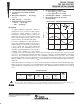
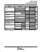
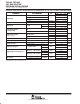
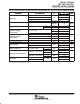
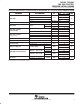
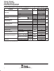
AVAILABLE OPTIONS
PACKAGED DEVICES
CHIP
T
A
SMALL
OUTLINE
(D)
CERAMIC
DIP
(JG)
PLASTIC
(LP)
PLASTIC
DIP
(P)
CHIP
FORM
(Y)
0°C to 70°C TLE2426CD — TLE2426CLP TLE2426CP
Please be aware that an important notice concerning availability, standard warranty, and use in critical applications o
f
Texas Instruments semiconductor products and disclaimers thereto appears at the end of this data sheet.
! " #$%! " &$'(#! )!%*
)$#!" # ! "&%##!" &% !+% !%" %," "!$%!"
"!)) -!.* )$#! &#%""/ )%" ! %#%""(. #($)%
!%"!/ (( &%!%"*
Copyright 1998, Texas Instruments Incorporated
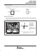
V
O
V
I
4
2
0
8
6
0 0.25 0.5 0.75 1
Voltage − V
t − Time − s
INPUT/OUTPUT TRANSFER CHARACTERISTICS
10
V
O
+
V
I
2
V
I
V
O