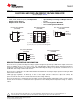
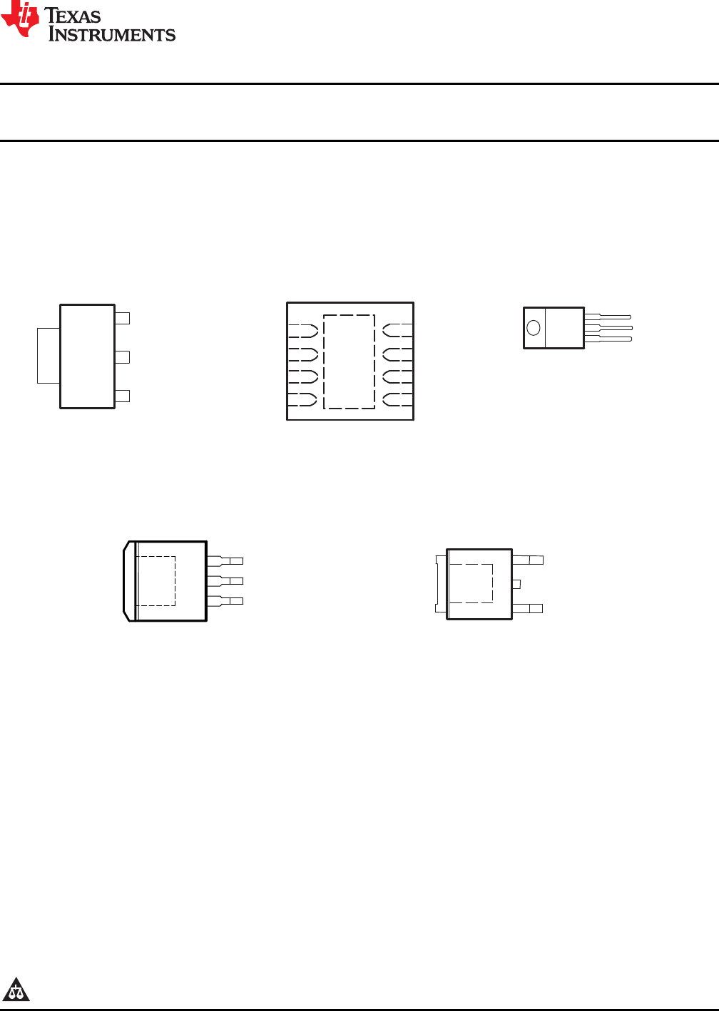
TLV1117 www.ti.com SLVS561K – DECEMBER 2004 – REVISED APRIL 2013 ADJUSTABLE AND FIXED LOW-DROPOUT VOLTAGE REGULATOR Check for Samples: TLV1117 FEATURES 1 • 1.5-V, 1.8-V, 2.5-V, 3.3-V, 5-V, and AdjustableOutput Voltage Options Output Current of 800 mA DCY (SOT-223) PACKAGE (TOP VIEW) OUTPUT INPUT OUTPUT ADJ/GND • • • Specified Dropout Voltage at Multiple Current Levels 0.2% Line Regulation Maximum 0.
TLV1117 SLVS561K – DECEMBER 2004 – REVISED APRIL 2013 www.ti.com These devices have limited built-in ESD protection. The leads should be shorted together or the device placed in conductive foam during storage or handling to prevent electrostatic damage to the MOS gates.
TLV1117 www.ti.
TLV1117 SLVS561K – DECEMBER 2004 – REVISED APRIL 2013 www.ti.
TLV1117 www.ti.com SLVS561K – DECEMBER 2004 – REVISED APRIL 2013 ABSOLUTE MAXIMUM RATINGS (1) over operating free-air temperature range (unless otherwise noted) MIN VIN Continuous input voltage TJ Operating virtual-junction temperature Tstg Storage temperature range (1) MAX –65 UNIT 16 V 150 °C 150 °C Stresses beyond those listed under "absolute maximum ratings" may cause permanent damage to the device.
TLV1117 SLVS561K – DECEMBER 2004 – REVISED APRIL 2013 www.ti.com TLV1117C ELECTRICAL CHARACTERISTICS TJ = 0°C to 125°C, all typical values are at TJ = 25°C (unless otherwise noted) TEST CONDITIONS (1) PARAMETER Reference voltage, VREF VIN – VOUT = 2 V, IOUT = 10 mA, TJ = 25°C VIN – VOUT = 1.4 V to 10 V, IOUT = 10 mA to 800 mA VIN = 3.5 V, IOUT = 10 mA, TJ = 25°C VIN = 2.9 V to 10 V, IOUT = 0 to 800 mA VIN = 3.8 V, IOUT = 10 mA, TJ = 25°C VIN = 3.2 V to 10 V, IOUT = 0 to 800 mA VIN = 4.
TLV1117 www.ti.com SLVS561K – DECEMBER 2004 – REVISED APRIL 2013 TLV1117I ELECTRICAL CHARACTERISTICS TJ = –40°C to 125°C, all typical values are at TJ = 25°C (unless otherwise noted) TEST CONDITIONS (1) PARAMETER Reference voltage, VREF VIN – VOUT = 2 V, IOUT = 10 mA, TJ = 25°C VIN – VOUT = 1.4 V to 10 V, IOUT = 10 mA to 800 mA VIN = 3.5 V, IOUT = 10 mA, TJ = 25°C VIN = 2.9 V to 10 V, IOUT = 0 to 800 mA VIN = 3.8 V, IOUT = 10 mA, TJ = 25°C VIN = 3.2 V to 10 V, IOUT = 0 to 800 mA VIN = 4.
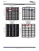
TLV1117 SLVS561K – DECEMBER 2004 – REVISED APRIL 2013 www.ti.com TYPICAL CHARACTERISTICS SHORT-CIRCUIT CURRENT vs (VIN – VOUT) LOAD REGULATION 0 1.8 TJ = 255C DLoad = 800 mA −0.05 1.4 TJ = 1255C −0.1 1.2 DVOUT (%) Short-Circuit Current (A) 1.6 1 0.8 −0.15 −0.2 0.6 −0.25 0.4 −0.3 0.2 0 0 3 6 9 12 −0.
TLV1117 www.ti.com SLVS561K – DECEMBER 2004 – REVISED APRIL 2013 TYPICAL CHARACTERISTICS (continued) ADJ PIN CURRENT vs TEMPERATURE 2 150 1.5 140 130 1 ADJ Pin Current (mA) 0.5 0 −0.5 −1 110 100 90 80 −1.5 −2 −50 120 70 −25 0 25 50 75 100 125 60 −50 150 Temperature (5C) TLV1117-33 LOAD TRANSIENT RESPONSE 0.2 2.6 100 2.4 90 1.8 1.6 1.4 −0.1 CIN = 10 mF COUT = 10-mF Tantalum −0.2 VIN = 4.8 V Preload = 0.1 A 1.2 1 0.8 0.6 −0.3 0.4 Load Current 0.2 −0.4 −0.
TLV1117 SLVS561K – DECEMBER 2004 – REVISED APRIL 2013 www.ti.com TYPICAL CHARACTERISTICS (continued) DROPOUT VOLTAGE vs LOAD CURRENT 1.4 1.2 TJ = 255C Dropout Voltage (V) 1 0.8 TJ = 1255C 0.6 0.4 0.
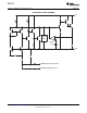
TLV1117 www.ti.com SLVS561K – DECEMBER 2004 – REVISED APRIL 2013 APPLICATION INFORMATION 1N4002 (See Note D) TLV1117 − ADJ INPUT VI OUTPUT VO ADJ/GND 10 µF (see Note C) IADJ VREF 100 µF (see Note A) CADJ (see Note B) VOUT is calculated as: ǒ R1 Ǔ VOUT + V REF 1 ) R2 ) (IADJ R1 R2 R2) Because IADJ typically is 55 µA, it is negligible in most applications. A. Output capacitor selection is critical for regulator stability.
TLV1117 SLVS561K – DECEMBER 2004 – REVISED APRIL 2013 www.ti.com REVISION HISTORY Changes from Revision J (April 2013) to Revision K • 12 Page Added additional package options. .......................................................................................................................................
PACKAGE OPTION ADDENDUM www.ti.
PACKAGE OPTION ADDENDUM www.ti.
PACKAGE OPTION ADDENDUM www.ti.
PACKAGE OPTION ADDENDUM www.ti.
PACKAGE OPTION ADDENDUM www.ti.
PACKAGE OPTION ADDENDUM www.ti.
PACKAGE OPTION ADDENDUM www.ti.com 31-Oct-2013 continues to take reasonable steps to provide representative and accurate information but may not have conducted destructive testing or chemical analysis on incoming materials and chemicals. TI and TI suppliers consider certain information to be proprietary, and thus CAS numbers and other limited information may not be available for release.
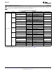
PACKAGE MATERIALS INFORMATION www.ti.com 12-Aug-2013 TAPE AND REEL INFORMATION *All dimensions are nominal Device TLV1117-15CDCYR Package Package Pins Type Drawing SPQ SOT-223 Reel Reel A0 Diameter Width (mm) (mm) W1 (mm) B0 (mm) K0 (mm) P1 (mm) W Pin1 (mm) Quadrant DCY 4 2500 330.0 12.4 7.05 7.4 1.9 8.0 12.0 Q3 TLV1117-15CDRJR SON DRJ 8 1000 180.0 12.4 4.25 4.25 1.15 8.0 12.0 Q2 TLV1117-15CKVURG3 TO-252 KVU 3 2500 330.0 16.4 6.9 10.5 2.7 8.0 16.
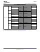
PACKAGE MATERIALS INFORMATION www.ti.com 12-Aug-2013 Device Package Package Pins Type Drawing SPQ Reel Reel A0 Diameter Width (mm) (mm) W1 (mm) TLV1117-33IDCYR SOT-223 DCY 4 2500 330.0 12.4 7.05 TLV1117-33IDRJR SON DRJ 8 1000 180.0 12.4 4.25 B0 (mm) K0 (mm) P1 (mm) W Pin1 (mm) Quadrant 7.4 1.9 8.0 12.0 Q3 4.25 1.15 8.0 12.0 Q2 TLV1117-33IKVURG3 TO-252 KVU 3 2500 330.0 16.4 6.9 10.5 2.7 8.0 16.0 Q2 TLV1117-50CDCYR SOT-223 DCY 4 2500 330.0 12.4 7.05 7.
PACKAGE MATERIALS INFORMATION www.ti.com 12-Aug-2013 *All dimensions are nominal Device Package Type Package Drawing Pins SPQ Length (mm) Width (mm) Height (mm) TLV1117-15CDCYR SOT-223 DCY 4 2500 340.0 340.0 38.0 TLV1117-15CDRJR SON DRJ 8 1000 210.0 185.0 35.0 TLV1117-15CKVURG3 TO-252 KVU 3 2500 340.0 340.0 38.0 TLV1117-15IDCYR SOT-223 DCY 4 2500 340.0 340.0 38.0 TLV1117-15IKVURG3 TO-252 KVU 3 2500 340.0 340.0 38.
MECHANICAL DATA MPDS094A – APRIL 2001 – REVISED JUNE 2002 DCY (R-PDSO-G4) PLASTIC SMALL-OUTLINE 6,70 (0.264) 6,30 (0.248) 3,10 (0.122) 2,90 (0.114) 4 0,10 (0.004) M 3,70 (0.146) 3,30 (0.130) 7,30 (0.287) 6,70 (0.264) Gauge Plane 1 2 0,84 (0.033) 0,66 (0.026) 2,30 (0.091) 4,60 (0.181) 1,80 (0.071) MAX 3 0°–10° 0,10 (0.004) M 0,25 (0.010) 0,75 (0.030) MIN 1,70 (0.067) 1,50 (0.059) 0,35 (0.014) 0,23 (0.009) Seating Plane 0,08 (0.003) 0,10 (0.0040) 0,02 (0.0008) 4202506/B 06/2002 NOTES: A. B.
MECHANICAL DATA MPFM001E – OCTOBER 1994 – REVISED JANUARY 2001 KTE (R-PSFM-G3) PowerFLEX PLASTIC FLANGE-MOUNT 0.375 (9,52) 0.080 (2,03) 0.070 (1,78) 0.365 (9,27) 0.360 (9,14) 0.050 (1,27) 0.040 (1,02) 0.350 (8,89) 0.220 (5,59) NOM 0.010 (0,25) NOM Thermal Tab (See Note C) 0.360 (9,14) 0.350 (8,89) 0.295 (7,49) NOM 0.320 (8,13) 0.310 (7,87) 0.420 (10,67) 0.410 (10,41) 1 3 0.025 (0,63) 0.031 (0,79) 0.100 (2,54) Seating Plane 0.004 (0,10) 0.010 (0,25) M 0.005 (0,13) 0.001 (0,03) 0.
MECHANICAL DATA MPSF001F – JANUARY 1996 – REVISED JANUARY 2002 KTP (R-PSFM-G2) PowerFLEX PLASTIC FLANGE-MOUNT PACKAGE 0.080 (2,03) 0.070 (1,78) 0.243 (6,17) 0.233 (5,91) 0.228 (5,79) 0.218 (5,54) 0.050 (1,27) 0.040 (1,02) 0.010 (0,25) NOM 0.130 (3,30) NOM 0.215 (5,46) NOM 0.247 (6,27) 0.237 (6,02) Thermal Tab (See Note C) 0.287 (7,29) 0.277 (7,03) 0.381 (9,68) 0.371 (9,42) 0.100 (2,54) 0.090 (2,29) 0.032 (0,81) MAX Seating Plane 0.090 (2,29) 0.180 (4,57) 0.004 (0,10) 0.005 (0,13) 0.
IMPORTANT NOTICE Texas Instruments Incorporated and its subsidiaries (TI) reserve the right to make corrections, enhancements, improvements and other changes to its semiconductor products and services per JESD46, latest issue, and to discontinue any product or service per JESD48, latest issue. Buyers should obtain the latest relevant information before placing orders and should verify that such information is current and complete.