User's Guide SLAU229B – October 2007 – Revised August 2008 TLV320AIC12KEVMB-K and TLV320AIC14KEVMB-K User's Guide This user's guide describes the characteristics, operation, and use of evaluation modules TLV320AIC12KEVMB and TLV320AIC14KEVMB, both as stand-alone and as kits (TLV320AIC12KEVMB-K and TLV320AIC14KEVMB-K). A complete circuit description, schematic diagram and bill of materials are also included. The following related documents are available through the Texas Instruments web site at www.ti.com.
www.ti.com 13 14 15 16 Command Line Interface Tab ............................................................................................ File Menu .................................................................................................................... Options Menu ............................................................................................................... Help ..............................................................................................................
EVM Overview www.ti.com 1 EVM Overview 1.1 Features • • • • • • • 1.2 Full-featured evaluation board for the TLV320AIC12K/14K audio codec TLV320AIC12KEVMB-K/14KEVMB-K features USB connectivity for quick and easy setup. Intuitive evaluation software Easy interfacing to multiple analog sources Analog output signals from the TLV320AIC12K/14K are available on top and bottom connectors.
Digital Interface www.ti.com Table 1. Analog Interface Pinout (continued) PIN NUMBER SIGNAL DESCRIPTION J2.2 INP2 Noninverting analog input 2 J2.3 NC Not Connected J2.4 NC Not Connected J2.5 NC Not Connected J2.6 NC Not Connected J2.7 INM1 Inverting analog input 1 J2.8 INP1 Noninverting analog input 1 J2.9 AGND Analog Ground J2.10 NC Not Connected J2.11 AGND Analog Ground J2.12 NC Not Connected J2.13 AGND Analog Ground J2.14 NC Not Connected J2.
Digital Interface www.ti.com Table 3. Digital Interface Pinout (continued) PIN NUMBER SIGNAL DESCRIPTION J4.6 NC Not Connected J4.7 NC Not Connected J4.8 AIC12K/14K RESET Reset signal input to AIC12K/14KEVMB J4.9 NC Not Connected J4.10 DGND Digital Ground J4.11 NC Not Connected J4.12 NC Not Connected J4.13 NC Not Connected J4.14 AIC12K/14K RESET Reset signal input to AIC12K/14KEVMB J4.15 NC Not Connected J4.16 SCL I2C Serial Clock J4.17 NC Not Connected J4.
Power Supplies 4 www.ti.com Power Supplies J3 provides connection to the common power bus for the TLV320AIC12KEVMB/14KEVMB. Power is supplied on the pins listed in Table 4. Table 4. Power Supply Pinout SIGNAL PIN NUMBER SIGNAL NC J3.1 J3.2 NC +5VA J3.3 J3.4 NC DGND J3.5 J3.6 AGND DVDD (1.8V) J3.7 J3.8 NC IOVDD (3.3V) J3.9 J3.10 NC The TLV320AIC12KEVMB-K/14KEVMB-K motherboard (the USB-MODEVM Interface board) supplies power to J3 of the TLV320AIC12KEVMB/14KEVMB.
Kit Operation www.ti.com 5.1 Analog Input The analog input sources can be applied directly to J2 (top or bottom side). The analog inputs may also be accessed through J8 and screw terminals J9 and J10. 5.2 Analog Output The analog outputs from the TLV320AIC12K/14K are available on J1 (top or bottom). They also may be accessed through J6 and J7 or J11. Note that the TLV320AIC14K only has one (differential) output which can be accessed from J1 or screw terminal J6. 5.
Kit Operation www.ti.com TLV320AIC12KEVMB/14KEVMB TLV320AIC12K/14K EVM Position 1 Control Interface I2C TAS1020B USB 8051 Microcontroller EVM Position 2 USB SMARTDM Audio Interface Figure 1. TLV320AIC12KEVMB-K/14KEVMB-K Block Diagram The USB-MODEVM Interface board is intended to be used in USB mode, where control of the installed EVM is accomplished using the onboard USB controller device. Provision is made, however, for driving all the data buses (I2C, PCM/SMARTDM™) externally.
Kit Operation www.ti.com Table 6.
Kit Operation www.ti.com Figure 2. Default Software Screen 6.3 USB-MODEVM Interface Board The simple diagram shown in Figure 1 shows only the basic features of the USB-MODEVM Interface board. The board is built around a TAS1020B streaming audio USB controller with an 8051-based core. The board features two positions for modular EVMs, or one double-wide serial modular EVM may be installed.
Kit Operation www.ti.com 6.5 Indicators and Main Screen Controls Figure 2 illustrates the indicators and the main screen controls near the top of the software screen display, and a large tabbed interface below. This section discusses the controls above this tabbed section. At the top left of the screen is an Interface indicator. The TLV320AIC12K/14K has an I2C interface. The indicator is lit after the program begins. Below the Interface indicator is the Device Connected indicator.
Kit Operation www.ti.com Figure 3. Information Tab Additionally, the operating system's audio device must be configured as AIC12K/14K EVM (see Figure 4). The External Audio Interface Configuration only allows I2C communication between the host computer and the TLV320AIC12K/14K. In this configuration, the TLV320AIC12K/14K can transmit and receive audio data to/from an external PCM device or DSP. SW2 on the USB-MODEVM must be configured as shown in the right section of Figure 3.
Kit Operation www.ti.com Figure 4. Sounds and Audio Devices Properties 6.7 Preset Configurations Tab The Preset Configurations tab (Figure 5) provides several presets for both the USB-MODEVM Audio Interface Configuration and the External Audio Interface Configuration. Also, there is a TLV320AIC12K/14K Defaults preset which programs the codec's default register settings. When a radio button is selected, a detailed description of the preset will appear on the Preset Configuration Description box.
Kit Operation www.ti.com Figure 5. Preset Configurations 6.8 Device Controls Tab The Device Controls Tab (Figure 6) contains six enumerated Control Registers sub tabs with controls for all six registers of the TLV320AIC12K/14K, a register table at the bottom of the tab, several controls and an indicator at the right of the tab. The 8-bit I2C Address indicator shows the current I2C address. The Device Position control lets the user select a specific codec on a master-slave chain to write to or read from.
Kit Operation www.ti.com Figure 6. Device Controls Tab 6.8.1 Control Register 1 Tab The Transfer Mode control lets the user select between continuous data transfer mode or programming mode. In the continuous data transfer mode, only audio data is sent and received through the serial audio bus. In the programming mode, control data is sent and received through the serial audio bus.
Kit Operation www.ti.com Figure 7. Control Register 1 Tab 6.8.2 Control Register 2 Tab The Turbo Mode control (Figure 8) sets the SCLK frequency to 16×FS×(number of devices)×mode or MCLK÷P, where number of devices is the number of codecs in cascade (default=1) and the mode is 1 for continuous data transfer mode and 2 for programming mode. The Host Port Control can be used to assign different functions to the SDA pin or to set SCL and SDA for I2C or S2C.
Kit Operation www.ti.com Figure 8. Control Register 2 Tab 6.8.3 Control Register 3 Tab The Control Register 3 Tab (Figure 9) allows the user to set the DAC Oversampling Rate (OSR), set the Asynchronous Sampling Rate Factor and power down the ADC or DAC with the Power Down Controls. The indicator below each power down switch will light when on only if the register data sent by pressing the Program Device button is acknowledged.
Kit Operation www.ti.com are merely for illustration; what is actually written to registers 4A and 4B are the values of P, M and N only. The USB-MODEVM Audio Interface Configuration is set up for an MCLK=11.2896 MHz, so P, M and N must satisfy the FS equation and the SCLK equation in Turbo Mode for that configuration. If using the External Audio Interface Configuration, the divider values can be set to anything specified in the TLV320AIC12K/14K datasheet. Figure 10. Control Register 4 Tab 6.8.
Kit Operation www.ti.com Please refer to Appendix A for details. Note that the ring contact in J8 is not connected. c. MICIN with external common mode (pseudo-differential) - In this mode, the single ended input is connected through ac-coupling to MICIN and the bias voltage used to generate the signal is also ac coupled to INM1. To use this mode, jumper W11 must be installed on pins 1-2.
Kit Operation www.ti.com Figure 13. Command Line Interface Tab A script is loaded into the command buffer, either by operating the controls on the other tabs or by loading a script file or preset. When executed, either by loading commands from other tabs, loading a preset or pushing the Execute Command Buffer button, an array containing executed commands will be displayed on the Command History tab.
Kit Operation www.ti.com Figure 14. File Menu The Options menu (Figure 15) provides two settings suitable for command line interface users and for troubleshooting. These settings allows the user to evaluate the device in its most basic form. The first option, Hardware Reset on Startup, enables (checked) and disables (unchecked) the hardware reset commands every time the GUI starts. If checked, a series of commands will be sent to the TAS1020 to hardware reset the TLV320AIC12K/14K at startup.
Kit Operation www.ti.com Figure 16. Help The actual USB protocol used as well as instructions on writing scripts are detailed in the following subsections. While it is not necessary to understand or use either the protocol or the scripts directly, understanding them may be helpful to some users. 6.9.1 USB-MODEVM Protocol The USB-MODEVM is defined to be a Vendor-Specific class, and is identified on the PC system as an NI-VISA device.
Kit Operation www.ti.com The data packet consists of the following bytes, shown in Table 8: Table 8. Data Packet Configuration BYTE NUMBER TYPE DESCRIPTION Specifies serial interface and operation. The two values are logically OR'd.
Kit Operation www.ti.
Kit Operation www.ti.com 6.9.1.1 GPIO Capability The USB-MODEVM has seven GPIO lines. The user can access them by specifying the interface to be 0x08, and then using the standard format for packets—but addresses are unnecessary. The GPIO lines are mapped into one byte (see Table 9): Table 9. GPIO Pin Assignments 7 6 5 4 3 2 1 0 x P3.5 P3.4 P3.3 P1.3 P1.2 P1.1 P1.0 Example: write P3.
Kit Operation 6.9.2 www.ti.com Writing Scripts A script is simply a text file that contains data to send to the serial control buses. The scripting language is quite simple, as is the parser for the language. Therefore, the program is not very forgiving about mistakes made in the source script file, but the formatting of the file is simple. Consequently, mistakes should be rare. Each line in a script file is one command. There is no provision for extending lines beyond one line.
Kit Operation www.ti.com 2 For example, to write the values 0x45 0xA0 to an I C device with a slave address of 0x80, starting at a register address of 0x01, one would write: #example script i i2cfast w 80 01 45 A0 r 80 01 02 This script begins with a comment, specifies that a fast I2C bus will be used, then writes 0x45 0xA0 to the I2C slave device at address 0x80, writing the values into registers 0x01 and 0x02. The script then reads back two bytes from the same device starting at register address 0x01.
Kit Operation www.ti.com Here is an example of a script: # # # # # # # # i w # d w # # i # # w # # r # # w # # w w # # # w w # # w # # w 28 TLV320AIC12K/14K This configuration allows playing audio to the DAC from any media player on a computer and recording from the ADC on audio recording software. Pin MICIN is configured as the input. The input can be heard via OUTP1/M1 and OUTP2/P3 due to the digital sidetone. Audio files played on the computer can also be heard via those outputs.
EVM Bill of Materials www.ti.com 7 EVM Bill of Materials Table 10 and Table 11 contain a complete bill of materials for the modular TLV320AIC12KEVMB/14KEVMB and the USB-MODEVM Interface Board. Table 10. TLV320AIC12KEVMB/14KEVMB Bill of Materials REFERENCE DESIGNATOR DESCRIPTION MANUFACTURER MFG PART NUMBER R7, R8 0Ω 1/10W 5% chip resistor Panasonic (or equivalent) ERJ-3GEY0R00V R5 2.
EVM Bill of Materials www.ti.com Table 11. USB-MODEVM Bill of Materials 30 Designators Description Manufacturer Mfg. Part Number R4 10Ω 1/10W 5% chip resistor Panasonic ERJ-3GEYJ100V R10, R11 27.
EVM Bill of Materials www.ti.com Table 11. USB-MODEVM Bill of Materials (continued) Designators Description Manufacturer Mfg. Part Number TP1, TP2, TP3, TP4, TP5, TP6, TP9, TP10, TP11 Miniature test point terminal Keystone Electronics 5000 TP7, TP8 Multipurpose test point terminal Keystone Electronics 5011 J7 USB type B slave connector thru-hole Mill-Max 897-30-004-90-000000 J1, J2, J3, J4, J5, J8 2-position terminal block On Shore Technology ED555/2DS J9 2.
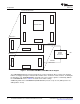
Appendix A www.ti.com Appendix A TLV320AIC12KEVMB/14KEVMB Schematic The schematic diagram is provided as a reference.
1 2 3 4 6 5 REVISION HISTORY REV J1A /J1B OUTM1 OUTMV D 1 3 5 7 9 11 13 15 17 19 A0(-) A1(-) A2(-) A3(-) AGND AGND AGND VCOM AGND AGND ENGINEERING CHANGE NUMBER APPROVED J4A /J4B A0(+) A1(+) A2(+) A3(+) A4 A5 A6 A7 REFREF+ 2 4 6 8 10 12 14 16 18 20 1 3 5 7 9 11 13 15 17 19 OUTP1 OUTP2 OUTMV OUTP3 PWDN CNTL CLKX CLKR FSX FSR DX DR INT TOUT GPIO5 GPIO0 DGND GPIO1 GPIO2 DGND GPIO3 GPIO4 SCL DGND SDA 2 4 6 8 10 12 14 16 18 20 W7 1 2 D RESET DAUGHTER-SERIAL DAUGHTER-ANALOG J1A (TOP) = SA
1 2 3 4 6 5 REVISION HISTORY REV 1 ENGINEERING CHANGE NUMBER APPROVED TP1 OUTP1 W10 2 OUTP1 IOVDD J6 1 R2 10K OUTP1 C5 0.1uF 2 D TP2 OUTM1 OUTM1 OUTM1 PWDN TP17 PWDN DIN TP18 DIN DOUT TP19 DOUT FS TP20 FS FSD TP21 FSD PWDN D IOVDD OUT1 J7 R3 10K +3.3VA OUTMV TP28 DRVSS W1 3 2 1 M/S TP11 AGND C18 R7 0 R1 1 W2 3 2 1 DVSS DVDD SCLK SDA SCL C15 W4 10uF 1 +1.8VD INP2 5 SCL 4 VSS WP C12 0.1uF C3 2 INM2 IN2 MCLK 0.
www.ti.com Appendix B Appendix B USB-MODEVM Schematic The schematic diagram is provided as a reference.
1 2 3 4 6 5 REVISION HISTORY REV ENGINEERING CHANGE NUMBER APPROVED D D USB Interface USB Interface Daughtercard Interface Daughtercard Interface MCLK BCLK LRCLK I2SDIN I2SDOUT MISO MOSI SS SCLK RESET INT PWR_DWN P3.3 P3.4 P3.5 P1.0 SDA SCL P1.1 P1.2 P1.3 C MCLK BCLK LRCLK I2SDIN I2SDOUT MISO MOSI SS SCLK RESET INT PWR_DWN P3.3 P3.4 P3.5 P1.0 SDA SCL P1.1 P1.2 P1.3 C B B ti A DATA ACQUISITION PRODUCTS HIGH-PERFORMANCE ANALOG DIVISION SEMICONDUCTOR GROUP 6730 SOUTH TUCSON BLVD.
1 2 3 4 6 5 REVISION HISTORY REV C33 +3.3VD +3.3VD APPROVED C41 0.1uF 5 1 IOVDD C32 ENGINEERING CHANGE NUMBER SDA C31 U11 VREF1 J6 1 3 SDA1 SCL1 GND EXTERNAL I2C 0.1uF 0.1uF USB I2S SN74AVC4T245PW PCA9306DCT +3.3VD 5 VCCB VCCA OE1 DIR1 OE2 DIR2 1B1 1A1 1B2 1A2 2B1 2A1 2B2 2A2 GND GND 0.1uF SCL C19 C C20 J7 USB SLAVE CONN 46 47 48 1 3 5 6 7 4 16 28 45 100pF GND D+ DVCC 4 3 2 1 C21 R9 1.5K R12 3.09K .001uF R10 27.
1 2 3 4 6 5 REVISION HISTORY REV ENGINEERING CHANGE NUMBER APPROVED D 1 2 3 D J11 J12 A0(-) A1(-) A2(-) A3(-) AGND AGND AGND VCOM AGND AGND 2 4 6 8 10 12 14 16 18 20 A0(+) A1(+) A2(+) A3(+) A4 A5 A6 A7 REFREF+ 1 3 5 7 9 11 13 15 17 19 +5VA DAUGHTER-ANALOG 1 3 5 7 9 +5VD JMP1 1 -VA -5VA AGND VD1 +5VD SCLK TP1 TP2 J12A (TOP) = SAM_TSM-110-01-L-DV-P J12B (BOTTOM) = SAM_SSW-110-22-F-D-VSIOVDD +5VD RESET IOVDD IOVDD C3 TP3 PWR_DWN 2 JMP3 R21 390 2.
FCC Warnings This equipment is intended for use in a laboratory test environment only. It generates, uses, and can radiate radio frequency energy and has not been tested for compliance with the limits of computing devices pursuant to subpart J of part 15 of FCC rules, which are designed to provide reasonable protection against radio frequency interference.
IMPORTANT NOTICE Texas Instruments Incorporated and its subsidiaries (TI) reserve the right to make corrections, modifications, enhancements, improvements, and other changes to its products and services at any time and to discontinue any product or service without notice. Customers should obtain the latest relevant information before placing orders and should verify that such information is current and complete.