
Datasheet
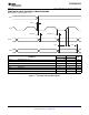

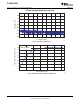

0.85
0.8
0.75
0.7
0.65
0.6
0.55
0.5
0.45
0.4
0 10 20 30 40 50 60 70
PGA Setting(dB)
GainError(dB)
Left ADC
Right ADC
G009
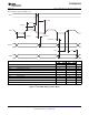
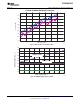
1.8
2.0
2.2
2.4
2.6
2.8
3.0
3.2
3.4
3.6
2.7 2.8 2.9 3.0 3.1 3.2 3.3 3.4 3.5 3.6
AVDD − Supply Voltage − V
MICBIAS Output Voltage − V
G007
MICBIAS = AVDD
MICBIAS = 2.5 V
MICBIAS = 2 V
TLV320AIC3105
www.ti.com
......................................................................................................................................... SLAS513B – FEBRUARY 2007 – REVISED DECEMBER 2008
TYPICAL CHARACTERISTICS (continued)
Figure 9. ADC Gain Error vs PGA Gain Setting
Figure 10. MICBIAS Output Voltage vs AVDD
Copyright © 2007 – 2008, Texas Instruments Incorporated Submit Documentation Feedback 17
Product Folder Link(s): TLV320AIC3105