
Datasheet
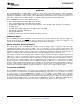
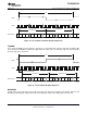
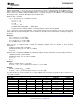

DA(6) DA(0) RA(7) RA(0) D(7) D(0)
T0147-01
SDA
SCL
(M) – SDA ControlledbyMaster
(S) – SDA ControlledbySlave
Start
(M)
Write
(M)
Slave
Ack
(S)
Slave
Ack
(S)
Slave
Ack
(S)
Stop
(M)
7-BitDevice Address
(M)
8-BitRegister Address
(M)
8-BitRegisterdata
(M)
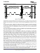
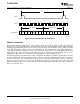
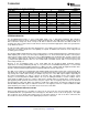
DA(6) DA(0) RA(7) RA(0)
SDA
SCL
DA(6) DA(0) D(7) D(0)
(M) – SDA ControlledbyMaster
(S) – SDA ControlledbySlave
Start
(M)
Write
(M)
Slave
Ack
(S)
Slave
Ack
(S)
Slave
Ack
(S)
Master
No Ack
(M)
Stop
(M)
Repeat
Start
(M)
Read
(M)
7-BitDevice Address
(M)
8-BitRegister Address
(M)
8-BitRegisterData
(S)
7-BitDevice Address
(M)
T0148-01
I
2
C BUS DEBUG IN A GLITCHED SYSTEM
DIGITAL AUDIO DATA SERIAL INTERFACE
TLV320AIC3105
www.ti.com
......................................................................................................................................... SLAS513B – FEBRUARY 2007 – REVISED DECEMBER 2008
The TLV320AIC3105 also responds to and acknowledges a General Call, which consists of the master issuing a
command with a slave address byte of 00H.
Figure 15. I
2
C Write
Figure 16. I
2
C Read
In the case of an I
2
C register write, if the master does not issue a STOP condition, then the device enters
auto-increment mode. So in the next eight clocks, the data on SDA is treated as data for the next incremental
register.
Similarly, in the case of an I
2
C register read, after the device has sent out the 8-bit data from the addressed
register, if the master issues an acknowledge, the slave takes over control of SDA bus and transmit for the next
8 clocks the data of the next incremental register.
Occasionally, some systems may encounter noise or glitches on the I
2
C bus. In the unlikely event that this
affects bus performance, then it can be useful to use the I
2
C Debug register. This feature terminates the I
2
C bus
error allowing this I
2
C device and system to resume communications. The I
2
C bus error detector is enabled by
default. The TLV320AIC3105 I
2
C error detector status can be read from page 0, register 107, bit D0. If desired,
the detector can be disabled by writing to page 0, register 107, bit D2.
Audio data is transferred between the host processor and the TLV320AIC3105 via the digital audio data serial
interface, or audio bus. The audio bus of the TLV320AIC3105 can be configured for left- or right-justified, I
2
S,
DSP, or TDM modes of operation, where communication with standard telephony PCM interfaces is supported
within the TDM mode. These modes are all MSB-first, with data width programmable as 16, 20, 24, or 32 bits. In
addition, the word clock (WCLK) and bit clock (BCLK) can be independently configured in either Master or Slave
mode, for flexible connectivity to a wide variety of processors
The word clock (WCLK) is used to define the beginning of a frame, and may be programmed as either a pulse or
a square-wave signal. The frequency of this clock corresponds to the maximum of the selected ADC and DAC
sampling frequencies.
Copyright © 2007 – 2008, Texas Instruments Incorporated Submit Documentation Feedback 23
Product Folder Link(s): TLV320AIC3105