
Datasheet

BCLK
WCLK
1 1
0 00
T0150-01
1/fs
LSBMSB
LeftChannel
RightChannel
2 2
SDIN/SDOUT
n–1 n–1 n–1n–2 n–2 n–2n–3 n–3
I
2
S MODE
BCLK
WCLK
1 1
0 0
T0151-01
1/fs
LSBMSB
LeftChannel
RightChannel
2 2
SDIN/SDOUT
n–1 n–1 n–1
1ClockBeforeMSB
n–2 n–2
n–3 n–3
DSP MODE
TLV320AIC3105
www.ti.com
......................................................................................................................................... SLAS513B – FEBRUARY 2007 – REVISED DECEMBER 2008
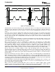
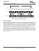
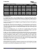
Figure 18. Left-Justified Serial Data Bus Mode Operation
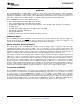
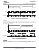
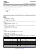
In I
2
S mode, the MSB of the left channel is valid on the second rising edge of the bit clock after the falling edge
of the word clock. Similarly the MSB of the right channel is valid on the second rising edge of the bit clock after
the rising edge of the word clock.
Figure 19. I
2
S Serial Data Bus Mode Operation
In DSP mode, the rising edge of the word clock starts the data transfer with the left-channel data first and
immediately followed by the right-channel data. Each data bit is valid on the falling edge of the bit clock.
Copyright © 2007 – 2008, Texas Instruments Incorporated Submit Documentation Feedback 25
Product Folder Link(s): TLV320AIC3105