
Datasheet

TLV320AIC3105
www.ti.com
......................................................................................................................................... SLAS513B – FEBRUARY 2007 – REVISED DECEMBER 2008
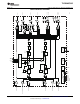
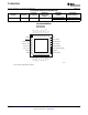
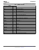
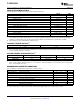
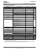
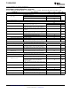
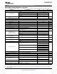
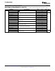
Table 1. TERMINAL FUNCTIONS
TERMINAL
DESCRIPTION
NAME QFN NO. I/O
AVDD 25 I Analog DAC voltage supply, 2.7 V – 3.6 V
AVSS1 17 I Analog ADC ground supply, 0 V
AVSS2 26 I Analog DAC ground supply, 0 V
BCLK 2 I/O Audio serial data bus bit clock input/output
DIN 4 I Audio serial data bus data input
DOUT 5 O Audio serial data bus data output
DRVDD 18 O Analog ADC and output driver voltage supply, 2.7 V – 3.6 V
DRVDD 24 O Analog output driver voltage supply, 2.7 V – 3.6 V
DRVSS 21 O Analog output driver ground supply, 0 V
DVDD 32 I Digital core voltage supply, 1.525 V – 1.95 V
DVSS 6 I/O Digital core / I/O ground supply, 0 V
HPLCOM 20 O High-power output driver (left – or multifunctional)
HPLOUT 19 O High-power output driver (left +)
HPRCOM 22 O High-power output driver (right – or multifunctional)
HPROUT 23 O High-power output driver (right +)
IOVDD 7 I/O Digital I/O voltage supply, 1.1 V – 3.6 V
LEFT_LOM 28 O Left line output ( – )
LEFT_LOP 27 O Left line output (+)
MCLK 1 I Master clock input
MIC1L/LINE1L 10 I Left input 1
MIC1R/LINE1R 11 I Right input 1
MIC2L/LINE2L 12 I Left input 2
MIC2R/LINE2R 13 I Right input 2
MIC3L/LINE3L/MICDET 14 I Left input 3; can support microphone detection
MIC3R/LINE3R 16 I Right input 3
MICBIAS 15 O Microphone bias voltage output
RESET 31 Reset
RIGHT_LOM 30 O Right line output ( – )
RIGHT_LOP 29 O Right line output (+)
SCL 8 I/O I
2
C serial clock input
SDA 9 I/O I
2
C serial data input/output
WCLK 3 I/O Audio serial data bus word clock input/output
Copyright © 2007 – 2008, Texas Instruments Incorporated Submit Documentation Feedback 5
Product Folder Link(s): TLV320AIC3105