
Datasheet

TLV320AIC3105
SLAS513B – FEBRUARY 2007 – REVISED DECEMBER 2008 .........................................................................................................................................
www.ti.com
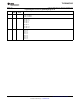
Page 0/Register 4: PLL Programming Register B
BIT READ/ RESET DESCRIPTION
WRITE VALUE
D7 – D2 R/W 0000 01 PLL J Value
0000 00: Reserved; do not write this sequence.
0000 01: J = 1
0000 10: J = 2
0000 11: J = 3
…
1111 10: J = 62
1111 11: J = 63
D1 – D0 R/W 00 Reserved. Write only zeros to these bits.
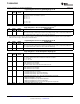
Page 0/Register 5: PLL Programming Register C
(1)
BIT READ/ RESET DESCRIPTION
WRITE VALUE
D7 – D0 R/W 0000 0000 PLL D value – Eight most significant bits of a 14-bit unsigned integer valid values for D are from zero to
9999, represented by a 14-bit integer located in Page-0/Reg-5 – Reg-6. Values should not be written into
these registers that would result in a D value outside the valid range.
(1) Note that whenever the D value is changed, register 5 should be written, immediately followed by register 6. Even if only the MSB or
LSB of the value changes, both registers should be written.
Page 0/Register 6: PLL Programming Register D
BIT READ/ RESET DESCRIPTION
WRITE VALUE
D7 – D2 R/W 0000 00 PLL D value – Six least significant bits of a 14-bit unsigned integer valid values for D are from zero to
9999, represented by a 14-bit integer located in Page-0/Reg-5 – Reg-6. Values should not be written into
these registers that would result in a D value outside the valid range.
D1 – D0 R 00 Reserved. Write only zeros to these bits.
Page 0/Register 7: Codec Datapath Setup Register
BIT READ/ RESET DESCRIPTION
WRITE VALUE
D7 R/W 0 f
S(ref)
Setting
This register setting controls timers related to the AGC time constants.
0: f
S(ref)
= 48 kHz
1: f
S(ref)
= 44.1 kHz
D6 R/W 0 ADC Dual-Rate Control
0: ADC dual-rate mode is disabled.
1: ADC dual-rate mode is enabled.
Note: ADC dual-rate mode must match DAC dual-rate mode.
D5 R/W 0 DAC Dual-Rate Control
0: DAC dual-rate mode is disabled.
1: DAC dual-rate mode is enabled.
D4 – D3 R/W 00 Left-DAC Data Path Control
00: Left-DAC data path is off (muted).
01: Left-DAC data path plays left-channel input data.
10: Left-DAC data path plays right channel input data.
11: Left-DAC data path plays mono mix of left- and right-channel input data.
D2 – D1 R/W 00 Right DAC Datapath Control
00: Right DAC datapath is off (muted).
01: Right DAC datapath plays right-channel input data.
10: Right DAC datapath plays left-channel input data.
11: Right DAC datapath plays mono mix of left- and right-channel input data.
D0 R/W 0 Reserved. Only write zero to this register.
50 Submit Documentation Feedback Copyright © 2007 – 2008, Texas Instruments Incorporated
Product Folder Link(s): TLV320AIC3105