
Datasheet
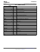
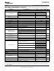

ABSOLUTE MAXIMUM RATINGS
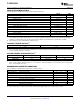
PACKAGE THERMAL RATINGS
(1)
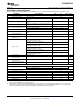
SYSTEM THERMAL CHARACTERISTICS
(1)
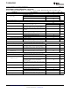
RECOMMENDED OPERATING CONDITIONS
TLV320AIC3105
SLAS513B – FEBRUARY 2007 – REVISED DECEMBER 2008 .........................................................................................................................................
www.ti.com
over operating free-air temperature range (unless otherwise noted)
(1) (2)
VALUE UNIT
AVDD to AVSS, DRVDD to DRVSS – 0.3 to 3.9 V
AVDD to DRVSS – 0.3 to 3.9 V
IOVDD to DVSS – 0.3 to 3.9 V
DVDD to DVSS – 0.3 to 2.5 V
AVDD to DRVDD – 0.1 to 0.1 V
Digital input voltage to DVSS – 0.3 to IOVDD + 0.3 V
Analog input voltage to AVSS – 0.3 to AVDD + 0.3 V
Operating temperature range – 40 to 85 ° C
Storage temperature range – 65 to 105 ° C
T
J
Max Junction temperature 105 ° C
Power dissipation (T
J
Max – T
A
)/ θ
JA
θ
JA
Thermal impedance 44 ° C/W
(1) Stresses beyond those listed under absolute maximum ratings may cause permanent damage to the device. These are stress ratings
only, and functional operation of the device at these or any other conditions beyond those indicated under recommended operating
conditions is not implied. Exposure to absolute-maximum-rated conditions for extended periods may affect device reliability.
(2) ESD complicance tested to EIA/JESD22-A114-B and passed.
PARAMETER TLV320AIC3105IRHB
R
θ JC
(1)
(C/W) 8.43
(1) R
θ JC
is the thermal resistance from junction to thermal pad. It is required to limit the power dissipation within the package to 500 mW in
all cases, including temperatures below 25 ° C.
Power Rating at 25 ° C, mW Power Rating, mW Derating Factor, ° C/W
High-K Board 500 500 at 80 ° C 48
Low-K Board 500 500 at 30 ° C 148
(1) It is required to limit the power dissipation within the package to 500 mW in all cases, including temperatures below 25 ° C. This data is
based on using a JEDEC standard four-layer 3-in. × 3-in. (7.62-mm × 7.62-mm) PCB with 2-oz. (0.071-mm thick) trace and copper pad
that is soldered directly to the device.
over operating free-air temperature range (unless otherwise noted)
MIN NOM MAX UNIT
AVDD, DRVDD1/2
(1)
Analog supply voltage 2.7 3.3 3.6 V
DVDD
(1)
Digital core supply voltage 1.525 1.8 1.95 V
IOVDD
(1)
Digital I/O supply voltage 1.1 1.8 3.6 V
V
I
Analog full-scale 0-dB input voltage (DRVDD1 = 3.3 V) 0.63 V
RMS
Stereo line output load resistance 10 k Ω
Stereo headphone output load resistance 16 Ω
Digital output load capacitance 10 pF
T
A
Operating free-air temperature – 40 85 ° C
(1) Analog voltage values are with respect to AVSS1, AVSS2, DRVSS; digital voltage values are with respect to DVSS.
6 Submit Documentation Feedback Copyright © 2007 – 2008, Texas Instruments Incorporated
Product Folder Link(s): TLV320AIC3105