
Datasheet


TLV320AIC3105
SLAS513B – FEBRUARY 2007 – REVISED DECEMBER 2008 .........................................................................................................................................
www.ti.com
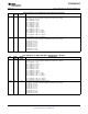
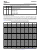
Page 0/Register 36: ADC Flag Register
BIT READ/ RESET DESCRIPTION
WRITE VALUE
D7 R 0 Left-ADC PGA Status
0: Applied gain and programmed gain are not the same.
1: Applied gain = programmed gain
D6 R 0 Left-ADC Power Status
0: Left ADC is in a power-down state.
1: Left ADC is in a power-up state.
D5 R 0 Left-AGC Signal Detection Status
0: Signal power is greater than noise threshold.
1: Signal power is less than noise threshold.
D4 R 0 Left-AGC Saturation Flag
0: Left AGC is not saturated.
1: Left-AGC gain applied = maximum allowed gain for left AGC
D3 R 0 Right ADC PGA Status
0: Applied gain and programmed gain are not the same.
1: Applied gain = programmed gain
D2 R 0 Right ADC Power Status
0: Right ADC is in a power-down state.
1: Right ADC is in a power-up state
D1 R 0 Right AGC Signal Detection Status
0: Signal power is greater than noise threshold.
1: Signal power is less than noise threshold.
D0 R 0 Right AGC Saturation Flag
0: Right AGC is not saturated
1: Right AGC gain applied = maximum allowed gain for right AGC
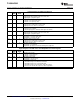
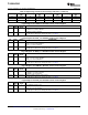
Page 0/Register 37: DAC Power and Output Driver Control Register
BIT READ/ RESET DESCRIPTION
WRITE VALUE
D7 R/W 0 Left-DAC Power Control
0: Left DAC is not powered up.
1: Left DAC is powered up.
D6 R/W 0 Right DAC Power Control
0: Right DAC is not powered up.
1: Right DAC is powered up.
D5 – D4 R/W 00 HPLCOM Output Driver Configuration Control
00: HPLCOM configured as differential of HPLOUT
01: HPLCOM configured as constant VCM output
10: HPLCOM configured as independent single-ended output
11: Reserved. Do not write this sequence to these register bits.
D3 – D0 R 000 Reserved. Write only zeros to these register bits.
62 Submit Documentation Feedback Copyright © 2007 – 2008, Texas Instruments Incorporated
Product Folder Link(s): TLV320AIC3105