
Datasheet


TLV320AIC3105
www.ti.com
......................................................................................................................................... SLAS513B – FEBRUARY 2007 – REVISED DECEMBER 2008
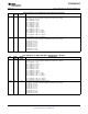
Page 0/Register 50: DAC_R1 to HPLOUT Volume Control Register
BIT READ/ RESET DESCRIPTION
WRITE VALUE
D7 R/W 0 DAC_R1 Output Routing Control
0: DAC_R1 is not routed to HPLOUT.
1: DAC_R1 is routed to HPLOUT.
D6 – D0 R/W 000 0000 DAC_R1 to HPLOUT Analog Volume Control
For 7-bit register setting versus analog gain values, see Table 6
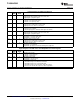
Page 0/Register 51: HPLOUT Output Level Control Register
BIT READ/ RESET DESCRIPTION
WRITE VALUE
D7 – D4 R/W 0000 HPLOUT Output Level Control
0000: Output level control = 0 dB
0001: Output level control = 1 dB
0010: Output level control = 2 dB
...
1000: Output level control = 8 dB
1001: Output level control = 9 dB
1010 – 1111: Reserved. Do not write these sequences to these register bits.
D3 R/W 0 HPLOUT Mute
0: HPLOUT is muted.
1: HPLOUT is not muted.
D2 R/W 1 HPLOUT Power-Down Drive Control
0: HPLOUT is weakly driven to a common-mode when powered down.
1: HPLOUT is high-impedance when powered down.
D1 R 1 HPLOUT Volume Control Status
0: All programmed gains to HPLOUT have been applied
1: Not all programmed gains to HPLOUT have been applied yet
D0 R/W 0 HPLOUT Power Control
0: HPLOUT is not fully powered up.
1: HPLOUT is fully powered up.
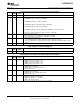
Page 0/Register 52: LINE2L to HPLCOM Volume Control Register
BIT READ/ RESET DESCRIPTION
WRITE VALUE
D7 R/W 0 LINE2L Output Routing Control
0: LINE2L is not routed to HPLCOM
1: LINE2L is routed to HPLCOM
D6 – D0 R/W 000 0000 LINE2L to HPLCOM Analog Volume Control
For 7-bit register setting versus analog gain values, see Table 6
Page 0/Register 53: PGA_L to HPLCOM Volume Control Register
BIT READ/ RESET DESCRIPTION
WRITE VALUE
D7 R/W 0 PGA_L Output Routing Control
0: PGA_L is not routed to HPLCOM
1: PGA_L is routed to HPLCOM
D6 – D0 R/W 000 0000 PGA_L to HPLCOM Analog Volume Control
For 7-bit register setting versus analog gain values, see Table 6
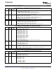
Page 0/Register 54: DAC_L1 to HPLCOM Volume Control Register
BIT READ/ RESET DESCRIPTION
WRITE VALUE
D7 R/W 0 DAC_L1 Output Routing Control
0: DAC_L1 is not routed to HPLCOM.
1: DAC_L1 is routed to HPLCOM.
D6 – D0 R/W 000 0000 DAC_L1 to HPLCOM Analog Volume Control
For 7-bit register setting versus analog gain values, see Table 6
Copyright © 2007 – 2008, Texas Instruments Incorporated Submit Documentation Feedback 67
Product Folder Link(s): TLV320AIC3105