
Datasheet


TLV320AIC3105
SLAS513B – FEBRUARY 2007 – REVISED DECEMBER 2008 .........................................................................................................................................
www.ti.com
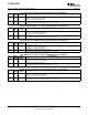
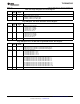
Page 0/Register 104: Left AGC New Programmable Decay Time Register
(1)
BIT READ/ RESET DESCRIPTION
WRITE VALUE
D7 R/W 0 Decay Time Register Selection
0: Decay time for the Left AGC is generated from register 26.
1: Decay time for the Left AGC is generated from this register.
D6 – D5 R/W 00 Baseline AGC Decay time
00: Left AGC Decay time = 50 ms
01: Left AGC Decay time = 150 ms
10: Left AGC Decay time = 250 ms
11: Left AGC Decay time = 350 ms
D4 – D2 R/W 000 Multiplication Factor for Baseline AGC
000: Multiplication factor for the baseline AGC Decay time = 1
001: Multiplication factor for the baseline AGC Decay time = 2
010: Multiplication factor for the baseline AGC Decay time = 4
011: Multiplication factor for the baseline AGC Decay time = 8
100: Multiplication factor for the baseline AGC Decay time = 16
101: Multiplication factor for the baseline AGC Decay time = 32
110: Multiplication factor for the baseline AGC Decay time = 64
111: Multiplication factor for the baseline AGC Decay time = 128
D1 – D0 R/W 00 Reserved. Write only zero to these register bits.
(1) Decay time is limited based on NADC ratio that is selected. For
NADC = 1, Maximum decay time = 4 seconds
NADC = 1.5, Maximum decay time = 5.6 seconds
NADC = 2, Maximum decay time = 8 seconds
NADC = 2.5, Maximum decay time = 9.6 seconds
NADC = 3 or 3.5, Maximum decay time = 11.2 seconds
NADC = 4 or 4.5, Maximum decay time = 16 seconds
NADC = 5, Maximum decay time = 19.2 seconds
NADC = 5.5 or 6, Maximum decay time = 22.4 seconds
In the TLV320AIC3105, the NDAC setting must be the same as the NADC setting. The NDAC ratio is set on page 0, register 2. The
NDAC is set equal to NADC by setting the value of bits D7 – D4 equal to that of bits D3 – D0.
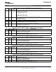
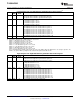
Page 0/Register 105: Right AGC New Programmable Attack Time Register
BIT READ/ RESET DESCRIPTION
WRITE VALUE
D7 R/W 0 Attack Time Register Selection
0: Attack time for the right AGC is generated from register 29.
1: Attack time for the right AGC is generated from this register.
D6 – D5 R/W 00 Baseline AGC attack time
00: Right AGC attack time = 7 ms
01: Right AGC attack time = 8 ms
10: Right AGC attack time = 10 ms
11: Right AGC attack time = 11 ms
D4 – D2 R/W 000 Multiplication Factor for Baseline AGC
000: Multiplication factor for the baseline AGC attack time = 1
001: Multiplication factor for the baseline AGC attack time = 2
010: Multiplication factor for the baseline AGC attack time = 4
011: Multiplication factor for the baseline AGC attack time = 8
100: Multiplication factor for the baseline AGC attack time = 16
101: Multiplication factor for the baseline AGC attack time = 32
110: Multiplication factor for the baseline AGC attack time = 64
111: Multiplication factor for the baseline AGC attack time = 128
D1 – D0 R/W 00 Reserved. Write only zero to these register bits.
78 Submit Documentation Feedback Copyright © 2007 – 2008, Texas Instruments Incorporated
Product Folder Link(s): TLV320AIC3105