
Datasheet


TLV320AIC3105
www.ti.com
......................................................................................................................................... SLAS513B – FEBRUARY 2007 – REVISED DECEMBER 2008
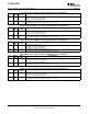
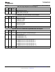
Page 0/Register 106: Right AGC New Programmable Decay Time Register
(1)
BIT READ/ RESET DESCRIPTION
WRITE VALUE
D7 R/W 0 Decay Time Register Selection
0: Decay time for the right AGC is generated from register 29.
1: Decay time for the right AGC is generated from this register.
D6 – D5 R/W 00 Baseline AGC Decay Time
00: Right AGC decay time = 50 ms
01: Right AGC Decay time = 150 ms
10: Right AGC Decay time = 250 ms
11: Right AGC Decay time = 350 ms
D4 – D2 R/W 000 Multiplication Factor for Baseline AGC
000: Multiplication factor for the baseline AGC decay time = 1
001: Multiplication factor for the baseline AGC decay time = 2
010: Multiplication factor for the baseline AGC decay time = 4
011: Multiplication factor for the baseline AGC decay time = 8
100: Multiplication factor for the baseline AGC decay time = 16
101: Multiplication factor for the baseline AGC decay time = 32
110: Multiplication factor for the baseline AGC decay time = 64
111: Multiplication factor for the baseline AGC decay time = 128
D1 – D0 R/W 00 Reserved. Write only zero to these register bits.
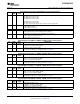
(1) Decay time is limited based on NADC ratio that is selected. For
NADC = 1, Maximum decay time = 4 seconds
NADC = 1.5, Maximum decay time = 5.6 seconds
NADC = 2, Maximum decay time = 8 seconds
NADC = 2.5, Maximum decay time = 9.6 seconds
NADC = 3 or 3.5, Maximum decay time = 11.2 seconds
NADC = 4 or 4.5, Maximum decay time = 16 seconds
NADC = 5, Maximum decay time = 19.2 seconds
NADC = 5.5 or 6, Maximum decay time = 22.4 seconds
In the TLV320AIC3105, the NDAC setting must be the same as the NADC setting. The NDAC ratio is set on page 0, register 2. The
NDAC is set equal to NADC by setting the value of bits D7 – D4 equal to that of bits D3 – D0.
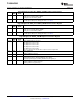
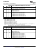
Page 0/Register 107: New Programmable ADC Digital Path and I
2
C Bus Condition Register
BIT READ/ RESET DESCRIPTION
WRITE VALUE
D7 R/W 0 Left Channel High-Pass Filter Coefficient Selection
0: Default coefficients are used when ADC high pass is enabled.
1: Programmable coefficients are used when ADC high pass is enabled.
D6 R/W 0 Right Channel High-Pass Filter Coefficient Selection
0: Default coefficients are used when ADC high pass is enabled.
1: Programmable coefficients are used when ADC high pass is enabled.
D5 – D4 R/W 00 ADC Decimation Filter Configuration
00: Left and right digital microphones are used.
01: Left digital microphone and right analog microphone are used.
10: Left analog microphone and right digital microphone are used.
11: Left and right analog microphones are used.
D3 R/W 0 ADC Digital Output to Programmable Filter Path Selection
0: No additional programmable filters other than the HPF are used for the ADC.
1: The programmable filter is connected to ADC output, if both DACs are powered down.
D2 R/W 0 I
2
C Bus Condition Detector
0: Internal logic is enabled to detect an I
2
C bus error, and clears the bus error condition.
1: Internal logic is disabled to detect an I
2
C bus hang.
D1 R 0 Reserved. Write only zero to these register bits.
D0 R 0 I
2
C Bus hang detection status
0: I
2
C bus hang is not detected
1: I
2
C bus hang is detected. This bit is cleared by reading this register.
Copyright © 2007 – 2008, Texas Instruments Incorporated Submit Documentation Feedback 79
Product Folder Link(s): TLV320AIC3105