
Datasheet


TLV320AIC3105
SLAS513B – FEBRUARY 2007 – REVISED DECEMBER 2008 .........................................................................................................................................
www.ti.com
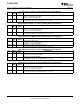
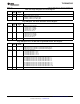
Page 0/Register 108: Passive Analog Signal Bypass Selection During Power Down Register
(1)
BIT READ/ RESET DESCRIPTION
WRITE VALUE
D7 R/W 0 Reserved. Only write a 0 to this bit.
D6 R/W 0 LINE2RP Path Selection
0: Normal Signal Path
1: Signal is routed by a switch to RIGHT_LOP
D5 R/W 0 Reserved. Only write a 0 to this bit.
D4 R/W 0 LINE1RP Path Selection
0: Normal Signal Path
1: Signal is routed by a switch to RIGHT_LOP
D3 R/W 0 Reserved. Only write a 0 to this bit.
D2 R/W 0 LINE2LP Path Selection
0: Normal Signal Path
1: Signal is routed by a switch to LEFT_LOP
D1 R/W 0 Reserved. Only write a 0 to this bit.
D0 R/W 0 LINE1LP Path Selection
0: Normal Signal Path
1: Signal is routed by a switch to LEFT_LOP
(1) Based on the setting above, if BOTH LINE1 and LINE2 inputs are routed to the output at the same time, then the two switches used for
the connection short the two input signals together on the output pins. The shorting resistance between the two input pins is two times
the bypass switch resistance (Rdson). In general, this condition of shorting should be avoided, as higher drive currents are likely to
occur on the circuitry that feeds these two input pins of this device.
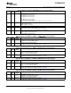
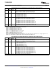
Page 0/Register 109: DAC Quiescent Current Adjustment Register
BIT READ/ RESET DESCRIPTION
WRITE VALUE
D7 – D6 R/W 00 DAC Current Adjustment
00: Default
01: 50% increase in DAC reference current
10: Reserved
11: 100% increase in DAC reference current
D5 – D0 R/W 00 0000 Reserved. Write only zeros to these register bits.
Page 0/Register 110 – 127: Reserved Registers
BIT READ/ RESET DESCRIPTION
WRITE VALUE
D7 – D0 R 0000 0000 Reserved. Do not write to these registers.
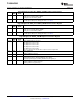
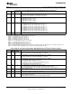
Page 1/Register 0: Page Select Register
BIT READ/ RESET DESCRIPTION
WRITE VALUE
D7 – D1 X 0000 000 Reserved. Write only zeros to these bits.
D0 R/W 0 Page Select Bit
Writing zero to this bit sets page 0 as the active page for following register accesses. Writing a one to this
bit sets page 1 as the active page for following register accesses. It is recommended that the user read
this register bit back after each write, to ensure that the proper page is being accessed for future register
read/writes. This register has the same functionality on page 0 and page 1.
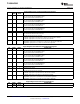
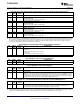
Page 1/Register 1: Left Channel Audio Effects Filter N0 Coefficient MSB Register
(1)
BIT READ/ RESET DESCRIPTION
WRITE VALUE
D7 – D0 R/W 0110 1011 Left-Channel Audio Effects Filter N0 Coefficient MSB
The 16-bit integer contained in the MSB and LSB registers for this coefficient are interpreted as a
2s-complement integer, with possible values ranging from – 32,768 to 32,767.
(1) When programming any coefficient value in Page 1, the MSB register should always be written first, immediately followed by the LSB
register. Even if only the MSB or LSB of the coefficient changes, both registers should be written in this sequence.
80 Submit Documentation Feedback Copyright © 2007 – 2008, Texas Instruments Incorporated
Product Folder Link(s): TLV320AIC3105