
Datasheet

EN
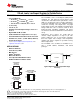
N/C
(1)
N/C
(1)
6
5
4
IN
GND
OUT
1
2
3
OUT
N/C
(1)
IN
GND
EN
1
2
3
5
4
OUT
N/C
(1)
IN
GND
EN
1
2
3 4
5
TLV700xx
www.ti.com
SLVSA00D –SEPTEMBER 2009–REVISED NOVEMBER 2012
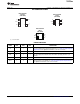
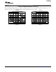
PIN CONFIGURATIONS
DDC PACKAGE
DCK PACKAGE
TSOT23-5
SC70-5
(TOP VIEW)
(TOP VIEW)
DSE PACKAGE
SON-6
(TOP VIEW)
(1) No connection.
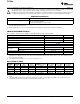
PIN DESCRIPTIONS
SON-6 SC70-5 TSOT23-5
NAME DSE DCK DDC DESCRIPTION
Input pin. A small 1-μF ceramic capacitor is recommended from this pin to ground
IN 1 1 1 to assure stability and good transient performance. See Input and Output Capacitor
Requirements in the Application Information section for more details.
GND 2 2 2 Ground pin
Enable pin. Driving EN over 0.9 V turns on the regulator. Driving EN below 0.4 V
EN 6 3 3 puts the regulator into shutdown mode and reduces operating current to 1 μA,
nominal.
NC 4, 5 4 4 No connection. This pin can be tied to ground to improve thermal dissipation.
Regulated output voltage pin. A small 1-μF ceramic capacitor is needed from this
OUT 3 5 5 pin to ground to assure stability. See Input and Output Capacitor Requirements in
the Application Information section for more details.
Copyright © 2009–2012, Texas Instruments Incorporated Submit Documentation Feedback 5