Product Folder Sample & Buy Technical Documents Tools & Software Support & Community F28M36P63C, F28M36P53C, F28M36H53C, F28M36H53B, F28M36H33C, F28M36H33B SPRS825C – OCTOBER 2012 – REVISED FEBRUARY 2014 F28M36x Concerto™ Microcontrollers 1 Device Summary 1.
F28M36P63C, F28M36P53C, F28M36H53C, F28M36H53B, F28M36H33C, F28M36H33B SPRS825C – OCTOBER 2012 – REVISED FEBRUARY 2014 1.2 • • • • Applications Servo Drives High-End AC Inverters Industrial UPS Solar Inverters 1.3 www.ti.com • • Electric Vehicle/Hybrid Electric Vehicle (EV/HEV) Chargers Power Line Communications Description The Concerto family is a multicore system-on-chip microcontroller unit (MCU) with independent communication and real-time control subsystems.
F28M36P63C, F28M36P53C, F28M36H53C, F28M36H53B, F28M36H33C, F28M36H33B www.ti.com 1.4 SPRS825C – OCTOBER 2012 – REVISED FEBRUARY 2014 Functional Block Diagram 1.8V VREG GPIO_MUX1 1.
F28M36P63C, F28M36P53C, F28M36H53C, F28M36H53B, F28M36H33C, F28M36H33B SPRS825C – OCTOBER 2012 – REVISED FEBRUARY 2014 www.ti.com Table of Contents 1 2 3 Device Summary ......................................... 1 5.1 Absolute Maximum Ratings 1.1 Features .............................................. 1 5.2 Handling Ratings................................... 123 1.2 Applications ........................................... 2 5.3 Recommended Operating Conditions 1.3 Description ................
F28M36P63C, F28M36P53C, F28M36H53C, F28M36H53B, F28M36H33C, F28M36H33B www.ti.com SPRS825C – OCTOBER 2012 – REVISED FEBRUARY 2014 2 Revision History NOTE: Page numbers for previous revisions may differ from page numbers in the current version. This data sheet revision history highlights the technical changes made to the SPRS825B device-specific data sheet to make it an SPRS825C revision.
F28M36P63C, F28M36P53C, F28M36H53C, F28M36H53B, F28M36H33C, F28M36H33B SPRS825C – OCTOBER 2012 – REVISED FEBRUARY 2014 www.ti.com 3 Device Overview The Concerto MCU comprises three subsystems: the Master Subsystem, the Control Subsystem, and the Analog Subsystem. While the Master and Control Subsystem each have dedicated local memories and peripherals, they can also share data and events through shared memories and peripherals. The Analog Subsystem has two ADC converters and six Analog Comparators.
F28M36P63C, F28M36P53C, F28M36H53C, F28M36H53B, F28M36H33C, F28M36H33B www.ti.com 3.1 SPRS825C – OCTOBER 2012 – REVISED FEBRUARY 2014 Device Characteristics Table 3-1 lists the features of the F28M36x devices. Table 3-1.
F28M36P63C, F28M36P53C, F28M36H53C, F28M36H53B, F28M36H33C, F28M36H33B SPRS825C – OCTOBER 2012 – REVISED FEBRUARY 2014 www.ti.com Table 3-1.
F28M36P63C, F28M36P53C, F28M36H53C, F28M36H53B, F28M36H33C, F28M36H33B www.ti.com SPRS825C – OCTOBER 2012 – REVISED FEBRUARY 2014 Table 3-1.
F28M36P63C, F28M36P53C, F28M36H53C, F28M36H53B, F28M36H33C, F28M36H33B SPRS825C – OCTOBER 2012 – REVISED FEBRUARY 2014 3.2 www.ti.com Memory Maps Section 3.2.1 shows the Control Subsystem Memory Map. Section 3.2.2 shows the Master Subsystem Memory Map. 3.2.1 Control Subsystem Memory Map Table 3-3.
F28M36P63C, F28M36P53C, F28M36H53C, F28M36H53B, F28M36H33C, F28M36H33B www.ti.com SPRS825C – OCTOBER 2012 – REVISED FEBRUARY 2014 Table 3-5.
F28M36P63C, F28M36P53C, F28M36H53C, F28M36H53B, F28M36H33C, F28M36H33B SPRS825C – OCTOBER 2012 – REVISED FEBRUARY 2014 www.ti.com Table 3-6.
F28M36P63C, F28M36P53C, F28M36H53C, F28M36H53B, F28M36H33C, F28M36H33B www.ti.com SPRS825C – OCTOBER 2012 – REVISED FEBRUARY 2014 Table 3-8.
F28M36P63C, F28M36P53C, F28M36H53C, F28M36H53B, F28M36H33C, F28M36H33B SPRS825C – OCTOBER 2012 – REVISED FEBRUARY 2014 www.ti.com Table 3-9.
F28M36P63C, F28M36P53C, F28M36H53C, F28M36H53B, F28M36H33C, F28M36H33B www.ti.com 3.2.2 SPRS825C – OCTOBER 2012 – REVISED FEBRUARY 2014 Master Subsystem Memory Map Table 3-10. Master Subsystem Flash, ECC, OTP, Boot ROM µDMA Access M Address (Byte-Aligned) (1) no 0000 0000 – 0000 FFFF Boot ROM - Dual-mapped to 0x0100 0000 (Both maps access same physical location.) 0001 0000 – 001F FFFF Reserved no 0020 0000 – 0020 7FFF Sector N (Zone 1 CSM password in the low address.
F28M36P63C, F28M36P53C, F28M36H53C, F28M36H53B, F28M36H33C, F28M36H33B SPRS825C – OCTOBER 2012 – REVISED FEBRUARY 2014 www.ti.com Table 3-10. Master Subsystem Flash, ECC, OTP, Boot ROM (continued) M Address (Byte-Aligned) (1) µDMA Access no Size (Bytes) Master Subsystem Flash, ECC, OTP, Boot ROM 0400 0000 – 07FF FFFF ROM/Flash/OTP/Boot ROM – Mirror-mapped for µCRC. Accessing this area of memory by the µCRC peripheral will cause an access in 0000 0000 – 03FF FFFF memory space.
F28M36P63C, F28M36P53C, F28M36H53C, F28M36H53B, F28M36H33C, F28M36H33B www.ti.com SPRS825C – OCTOBER 2012 – REVISED FEBRUARY 2014 Table 3-11.
F28M36P63C, F28M36P53C, F28M36H53C, F28M36H53B, F28M36H33C, F28M36H33B SPRS825C – OCTOBER 2012 – REVISED FEBRUARY 2014 www.ti.com Table 3-12.
F28M36P63C, F28M36P53C, F28M36H53C, F28M36H53B, F28M36H33C, F28M36H33B www.ti.com SPRS825C – OCTOBER 2012 – REVISED FEBRUARY 2014 Table 3-12.
F28M36P63C, F28M36P53C, F28M36H53C, F28M36H53B, F28M36H33C, F28M36H33B SPRS825C – OCTOBER 2012 – REVISED FEBRUARY 2014 www.ti.com Table 3-13.
F28M36P63C, F28M36P53C, F28M36H53C, F28M36H53B, F28M36H33C, F28M36H33B www.ti.com 3.3 SPRS825C – OCTOBER 2012 – REVISED FEBRUARY 2014 Master Subsystem The Master Subsystem includes the Cortex-M3 CPU, µDMA, Nested Vectored Interrupt Controller (NVIC), Cortex-M3 Peripherals, and Local Memory. Additionally, the Cortex-M3 CPU and µDMA can access the Control Subsystem through Shared Resources: IPC (CPU only), Message RAM, and Shared RAM; and read ADC Result Registers via the Analog Common Interface Bus.
F28M36P63C, F28M36P53C, F28M36H53C, F28M36H53B, F28M36H33C, F28M36H33B SPRS825C – OCTOBER 2012 – REVISED FEBRUARY 2014 www.ti.
F28M36P63C, F28M36P53C, F28M36H53C, F28M36H53B, F28M36H33C, F28M36H33B www.ti.com 3.3.2 SPRS825C – OCTOBER 2012 – REVISED FEBRUARY 2014 Cortex-M3 DMA and NVIC The Cortex-M3 direct memory access (µDMA) module provides a hardware method of transferring data between peripherals, between memory, and between peripherals and memory without intervention from the Cortex-M3 CPU. The NVIC manages and prioritizes interrupt handling for the Cortex-M3 CPU.
F28M36P63C, F28M36P53C, F28M36H53C, F28M36H53B, F28M36H33C, F28M36H33B SPRS825C – OCTOBER 2012 – REVISED FEBRUARY 2014 www.ti.com Table 3-15. Interrupts from NVIC to Cortex-M3 (continued) Interrupt Number (Bit in Interrupt Registers) 24 Vector Number Vector Address or Offset Description 37 53 0x0000.00D4 38–41 54–57 – I2C1 42 58 0x0000.00E8 Ethernet Controller 44 60 0x0000.00F0 USB 45 61 – 46 62 0x0000.00F8 µDMA Software 47 63 0x0000.
F28M36P63C, F28M36P53C, F28M36H53C, F28M36H53B, F28M36H33C, F28M36H33B www.ti.com SPRS825C – OCTOBER 2012 – REVISED FEBRUARY 2014 Table 3-15. Interrupts from NVIC to Cortex-M3 (continued) Interrupt Number (Bit in Interrupt Registers) Vector Number Vector Address or Offset 132 148 0x0000.0250 GPIO Port R 133 149 0x0000.0254 GPIO Port S Description Table 3-16.
F28M36P63C, F28M36P53C, F28M36H53C, F28M36H53B, F28M36H33C, F28M36H33B SPRS825C – OCTOBER 2012 – REVISED FEBRUARY 2014 3.3.4 www.ti.com Cortex-M3 Vector Table Each peripheral interrupt of Table 3-15 is assigned an address offset containing the location of the peripheral interrupt handler (relative to the vector table base) for that particular interrupt (vector numbers 16–107).
F28M36P63C, F28M36P53C, F28M36H53C, F28M36H53B, F28M36H33C, F28M36H33B www.ti.com 3.3.7 SPRS825C – OCTOBER 2012 – REVISED FEBRUARY 2014 Cortex-M3 Accessing Shared Resources and Analog Peripherals There are several memories, digital peripherals, and analog peripherals that can be accessed by both the Master and Control Subsystems. They are grouped into Shared Resources and the Analog Subsystem.
F28M36P63C, F28M36P53C, F28M36H53C, F28M36H53B, F28M36H33C, F28M36H33B SPRS825C – OCTOBER 2012 – REVISED FEBRUARY 2014 www.ti.
F28M36P63C, F28M36P53C, F28M36H53C, F28M36H53B, F28M36H33C, F28M36H33B www.ti.com 3.4.1 SPRS825C – OCTOBER 2012 – REVISED FEBRUARY 2014 C28x CPU/FPU/VCU The F28M36x Concerto MCU family is a member of the TMS320C2000 MCU platform. The Concerto C28x CPU/FPU has the same 32-bit fixed-point architecture as TI's existing Piccolo MCUs, combined with a single-precision (32-bit) IEEE 754 FPU of TI’s existing Delfino MCUs.
F28M36P63C, F28M36P53C, F28M36H53C, F28M36H53B, F28M36H33C, F28M36H33B SPRS825C – OCTOBER 2012 – REVISED FEBRUARY 2014 www.ti.com Table 3-17. PIE Peripheral Interrupts (1) PIE INTERRUPTS CPU INTERRUPTS (1) INTx.8 INTx.7 INTx.6 INTx.5 INTx.4 INTx.3 INTx.2 INTx.1 INT1 C28.
F28M36P63C, F28M36P53C, F28M36H53C, F28M36H53B, F28M36H33C, F28M36H33B www.ti.com 3.4.5 SPRS825C – OCTOBER 2012 – REVISED FEBRUARY 2014 C28x Local Peripherals The C28x local peripherals include an NMI Watchdog, three Timers, four Serial Port Peripherals (SCI, SPI, McBSP, I2C), an EPI, and three types of Control Peripherals (ePWM, eQEP, eCAP). All peripherals are accessible by the C28x CPU via the C28x Memory Bus. Additionally, the McBSP and ePWM are accessible by the C28x DMA Bus.
F28M36P63C, F28M36P53C, F28M36H53C, F28M36H53B, F28M36H33C, F28M36H33B SPRS825C – OCTOBER 2012 – REVISED FEBRUARY 2014 3.5 www.ti.com Analog Subsystem The Analog Subsystem has ADC1, ADC2, and six Analog Comparator + DAC units that can be accessed via the Analog Common Interface Bus. The ADC Result Registers are accessible by CPUs and DMAs of the Master and Control Subsystems. All other Analog Peripheral Registers are accessible by the C28x CPU only.
F28M36P63C, F28M36P53C, F28M36H53C, F28M36H53B, F28M36H33C, F28M36H33B www.ti.
F28M36P63C, F28M36P53C, F28M36H53C, F28M36H53B, F28M36H33C, F28M36H33B SPRS825C – OCTOBER 2012 – REVISED FEBRUARY 2014 3.5.3 www.ti.com Analog Comparator + DAC There are six Comparator blocks enabling simultaneous comparison of multiple pairs of analog inputs, resulting in six digital comparison outputs. The external analog inputs that are being compared in the comparators come from AIO_MUX1 and AIO_MUX2 blocks.
F28M36P63C, F28M36P53C, F28M36H53C, F28M36H53B, F28M36H33C, F28M36H33B www.ti.com 3.6 SPRS825C – OCTOBER 2012 – REVISED FEBRUARY 2014 Master Subsystem NMIs The Cortex-M3 NMI Block generates an M3NMIINT non-maskable interrupt to the Cortex-M3 CPU and an M3NMI event to the NMI Watchdog in response to potentially critical conditions existing inside or outside the Concerto MCU. When able to respond to the M3NMIINT interrupt, the Cortex-M3 CPU may address the NMI condition and disable the NMI Watchdog.
F28M36P63C, F28M36P53C, F28M36H53C, F28M36H53B, F28M36H33C, F28M36H33B SPRS825C – OCTOBER 2012 – REVISED FEBRUARY 2014 www.ti.com M3 BIST 1.
F28M36P63C, F28M36P53C, F28M36H53C, F28M36H53B, F28M36H33C, F28M36H33B www.ti.com 3.8 SPRS825C – OCTOBER 2012 – REVISED FEBRUARY 2014 Resets The Concerto MCU has two external reset pins: XRS for the Master and Control Subsystems and ARS for the Analog Subsystem. Texas Instruments (TI) recommends that these two pins be externally tied together with a board signal trace.
F28M36P63C, F28M36P53C, F28M36H53C, F28M36H53B, F28M36H33C, F28M36H33B SPRS825C – OCTOBER 2012 – REVISED FEBRUARY 2014 www.ti.
F28M36P63C, F28M36P53C, F28M36H53C, F28M36H53B, F28M36H33C, F28M36H33B www.ti.com 3.8.2 SPRS825C – OCTOBER 2012 – REVISED FEBRUARY 2014 C28x Resets The C28x CPU is reset by the C28RSTIN signal, and the C28x CPU in turn resets the rest of the C28x Subsystem with the C28SYSRST signal. When reset, the C28x restarts program execution from the address provided at the top of the Boot ROM Vector Table. The C28RSTIN has five possible sources: XRS, C28NMIWD, M3SWRST, M3DBGRST, and the M3RSNIN.
F28M36P63C, F28M36P53C, F28M36H53C, F28M36H53B, F28M36H33C, F28M36H33B SPRS825C – OCTOBER 2012 – REVISED FEBRUARY 2014 www.ti.com Table 3-18.
F28M36P63C, F28M36P53C, F28M36H53C, F28M36H53B, F28M36H33C, F28M36H33B www.ti.com SPRS825C – OCTOBER 2012 – REVISED FEBRUARY 2014 If the boot pins are set to 0010b, the application code will be loaded from the Master Subsystem UART0, SSI0, or I2C0 peripheral. (SSI0 and I2C0 are configured to work in Slave mode in this Boot Mode.) If the boot pins are set to 0011b, the application code will be loaded from the Master Subsystem CAN interface.
F28M36P63C, F28M36P53C, F28M36H53C, F28M36H53B, F28M36H33C, F28M36H33B SPRS825C – OCTOBER 2012 – REVISED FEBRUARY 2014 www.ti.com The boot process can be considered completed once the Cortex-M3 and C28x are both running out of their respective application programs.
F28M36P63C, F28M36P53C, F28M36H53C, F28M36H53B, F28M36H33C, F28M36H33B www.ti.com SPRS825C – OCTOBER 2012 – REVISED FEBRUARY 2014 CONNECT THE 2 RESET PINS EXTERNALLY THROUGH A BOARD TRACE ARS PIN XRS PIN CONCERTO DEVICE M3WDOGS ARS XRS DE-GLITCH DE-GLITCH ‘0’ ‘0’ POWER-ON-RESET (DIGITAL SUBSYSTEM) 1.8V POR 3.3V POR 1.8V TRISTATE 3.3V POR 3.3V POR 1.2V 1.
F28M36P63C, F28M36P53C, F28M36H53C, F28M36H53B, F28M36H33C, F28M36H33B SPRS825C – OCTOBER 2012 – REVISED FEBRUARY 2014 3.9.2 www.ti.com Digital Subsystem's Internal 1.2-V VREG The internal 1.2-V VREG generates VDD12 power from VDDIO. The 1.2-V VREG is enabled by pulling the VREG12EN pin to a low state. When enabled, the 1.2-V VREG internally provides 1.2 V to digital logic associated with the processors, memory, and peripherals of the Digital Subsystem. When the internal 1.
F28M36P63C, F28M36P53C, F28M36H53C, F28M36H53B, F28M36H33C, F28M36H33B www.ti.com SPRS825C – OCTOBER 2012 – REVISED FEBRUARY 2014 3.10 Input Clocks and PLLs Concerto devices have multiple input clock pins from which all internal clocks and the output clock are derived. Figure 3-7 shows the recommended methods of connecting crystals, resonators, and oscillators to pins X1/X2 and XCLKIN.
F28M36P63C, F28M36P53C, F28M36H53C, F28M36H53B, F28M36H33C, F28M36H33B SPRS825C – OCTOBER 2012 – REVISED FEBRUARY 2014 www.ti.com 3.10.2 Crystal Oscillator/Resonator (Pins X1/X2 and VSSOSC) The main oscillator circuit connects to an external crystal through pins X1 and X2. If a resonator is used (version of a crystal with built-in load capacitors), its ground terminal should be connected to the pin VSSOSC (not board ground).
F28M36P63C, F28M36P53C, F28M36H53C, F28M36H53B, F28M36H33C, F28M36H33B www.ti.com SPRS825C – OCTOBER 2012 – REVISED FEBRUARY 2014 SYSPLLMULT REG SPLLIMULT SYSPLLCTL REG SPLLFMULT SPLLEN (2) SYSDIVSEL REG SPLLCLKEN OSCCLK 7 SYSDIVSEL (1:0) = 00 ( /1 ) 0 2 /1 /2 /4 /8 MAIN PLL PIN X1 INTEGER MULTIPLIER MAIN OSC FRACTIONAL MULTIPLIER /2 OSCCLK 0000000 : 0000001 : 0000010 : 0000011 : . . . x x x x 1 1 2 3 00: NOT USED 01: x 0.25 10: x 0.50 11: x 0.
F28M36P63C, F28M36P53C, F28M36H53C, F28M36H53B, F28M36H33C, F28M36H33B SPRS825C – OCTOBER 2012 – REVISED FEBRUARY 2014 www.ti.com Table 3-20.
F28M36P63C, F28M36P53C, F28M36H53C, F28M36H53B, F28M36H33C, F28M36H33B www.ti.com SPRS825C – OCTOBER 2012 – REVISED FEBRUARY 2014 Table 3-21.
F28M36P63C, F28M36P53C, F28M36H53C, F28M36H53B, F28M36H33C, F28M36H33B SPRS825C – OCTOBER 2012 – REVISED FEBRUARY 2014 www.ti.com Table 3-22.
F28M36P63C, F28M36P53C, F28M36H53C, F28M36H53B, F28M36H33C, F28M36H33B www.ti.com SPRS825C – OCTOBER 2012 – REVISED FEBRUARY 2014 Table 3-23.
F28M36P63C, F28M36P53C, F28M36H53C, F28M36H53B, F28M36H33C, F28M36H33B SPRS825C – OCTOBER 2012 – REVISED FEBRUARY 2014 www.ti.com UPLLMULT REG UPLLCLKSRC UPLLIMULT UPLLCTL REG UPLLFMULT UPLLEN (2) UPLLCLKEN 0 6 2 PIN X1 USB PLL MAIN OSC OSCCLK 0 INTEGER MULTIPLIER /4 PLLINP XCLKIN USBPLLCLK FRACTIONAL MULTIPLIER 000000 : 000001 : 000010 : 000011 : . . . 1 PIN XCLKIN x x x x 1 1 2 3 00: NOT USED 01: x 0.25 10: x 0.50 11: x 0.
F28M36P63C, F28M36P53C, F28M36H53C, F28M36H53B, F28M36H33C, F28M36H33B www.ti.com SPRS825C – OCTOBER 2012 – REVISED FEBRUARY 2014 Table 3-24.
F28M36P63C, F28M36P53C, F28M36H53C, F28M36H53B, F28M36H33C, F28M36H33B SPRS825C – OCTOBER 2012 – REVISED FEBRUARY 2014 www.ti.com Table 3-25.
F28M36P63C, F28M36P53C, F28M36H53C, F28M36H53B, F28M36H33C, F28M36H33B www.ti.com SPRS825C – OCTOBER 2012 – REVISED FEBRUARY 2014 3.11 Master Subsystem Clocking The internal PLLSYSCLK clock, normally used as a source for all Master Subsystem clocks, is a divideddown output of the Main PLL or X1 external clock input, as defined by the SPLLCKEN bit of the SYSPLLCTL register. There is also a second oscillator that internally generates two clocks: 32KHZCLK and 10MHZCLK.
F28M36P63C, F28M36P53C, F28M36H53C, F28M36H53B, F28M36H33C, F28M36H33B SPRS825C – OCTOBER 2012 – REVISED FEBRUARY 2014 www.ti.
F28M36P63C, F28M36P53C, F28M36H53C, F28M36H53B, F28M36H33C, F28M36H33B www.ti.com SPRS825C – OCTOBER 2012 – REVISED FEBRUARY 2014 PLLSYSCLK 150 MHz Max OSCCLK System PLL /1 /1 /2 0* /2 /4* 1 /4 /8* XPLLCLKOUT Pin 100 MHz Max /1 Master (M3) Subsystem /2 /4* M3 Read/Write C28 Read Only** 150 MHz Max /1 on* 0 off Control (C28) Subsystem M3 Read/Write 0 XTAL X1 X2 0* 1 off XTAL OSC XCLKIN /1 37.5 MHz Max /2 Analog /4 /8* X1/X2 Ext. XTAL 4 – 20 MHz X1 Ext.
F28M36P63C, F28M36P53C, F28M36H53C, F28M36H53B, F28M36H33C, F28M36H33B SPRS825C – OCTOBER 2012 – REVISED FEBRUARY 2014 www.ti.com 3.11.1 Cortex-M3 Run Mode In Run Mode, the Cortex-M3 processor, memory, and most of the peripherals are clocked by the M3SSCLK, which is a divide-down version of the PLLSYSCLK (from Main PLL). The USB is clocked from a dedicated USB PLL, the CAN peripherals are clocked by M3SSCLK, OSCCLK, or XCLKIN, and one of two watchdogs (WDOG1) is also clocked by the OSCCLK.
F28M36P63C, F28M36P53C, F28M36H53C, F28M36H53B, F28M36H33C, F28M36H33B www.ti.com SPRS825C – OCTOBER 2012 – REVISED FEBRUARY 2014 3.11.3 Cortex-M3 Deep Sleep Mode In Deep Sleep Mode, the Cortex-M3 processor and memory are prevented from clocking and thus the code is no longer executing. The Main PLL, USB PLL, ASYSCLK to the Analog Subsystem, and input clock to the C28x CPU and Shared Resources are turned off. The gating for the peripheral clocks may change based on the ACG bit of the RCC register.
F28M36P63C, F28M36P53C, F28M36H53C, F28M36H53B, F28M36H33C, F28M36H33B SPRS825C – OCTOBER 2012 – REVISED FEBRUARY 2014 www.ti.com 3.12 Control Subsystem Clocking The CLKIN input clock to the C28x processor is normally a divided-down output of the Main PLL or X1 external clock input. There are four registers associated with the Main PLL: SYSPLLCTL, SYSPLLMULT, SYSPLLSTAT and SYSDIVSEL. Typically, the Cortex-M3 processor writes to these registers, while the C28x processor has read access.
F28M36P63C, F28M36P53C, F28M36H53C, F28M36H53B, F28M36H33C, F28M36H33B www.ti.
F28M36P63C, F28M36P53C, F28M36H53C, F28M36H53B, F28M36H33C, F28M36H33B SPRS825C – OCTOBER 2012 – REVISED FEBRUARY 2014 www.ti.com 3.12.3 C28x STANDBY Mode In STANDBY Mode, the C28x processor stops executing instructions and the C28CLKIN, C28CPUCLK, and C28SYSCLK are turned off. Exit from STANDBY Mode is accomplished by one of 64 GPIOs from the GPIO_MUX1 block, or MTOCIPCINT1 (interrupt from MTOC IPC peripheral).
F28M36P63C, F28M36P53C, F28M36H53C, F28M36H53B, F28M36H33C, F28M36H33B www.ti.com SPRS825C – OCTOBER 2012 – REVISED FEBRUARY 2014 3.13 Analog Subsystem Clocking The Analog Subsystem is clocked by ASYSCLK, which is a divided-down version of the PLLSYSCLK as defined by CLKDIV bits of the CCLKCTL register. The CCLKCTL register is exclusively accessible by the C28x processor. The CCLKCTL register is reset by ASYSRST, which is derived from two Analog Subsystem resets—ACIBRST and SRXRST.
F28M36P63C, F28M36P53C, F28M36H53C, F28M36H53B, F28M36H33C, F28M36H33B SPRS825C – OCTOBER 2012 – REVISED FEBRUARY 2014 X2 PIN www.ti.
F28M36P63C, F28M36P53C, F28M36H53C, F28M36H53B, F28M36H33C, F28M36H33B www.ti.com SPRS825C – OCTOBER 2012 – REVISED FEBRUARY 2014 3.16 GPIOs and Other Pins Most Concerto external pins are shared among many internal peripherals. This sharing of pins is accomplished through several I/O muxes where a specific physical pin can be assigned to selected signals of internal peripherals. Most of the I/O pins of the Concerto MCU can also be configured as programmable GPIOs.
F28M36P63C, F28M36P53C, F28M36H53C, F28M36H53B, F28M36H33C, F28M36H33B SPRS825C – OCTOBER 2012 – REVISED FEBRUARY 2014 12 AIO_MUX1 MII TX1 MII TX0 MII TX2 MII TX3 MII TXEN MII MDC MII PHYRSTN MII TXER MII MDIO MII PHYINTRN MII CRS MII COL MII RXCK MII TXCK MII RXDV MII RXER MII RX0 MII RX2 MII RX1 UART (5) NVIC CAN (2) 2 SSI (4) IC (2) I2C (1:0) SCL I2C (1:0) SDA SSI (3:0) RX SSI (3:0) TX SSI (3:0) CLK SSI (3:0) FSS XCLKIN GPIO CAN (1:0) TX CAN (1:0) RX GPIO_MUX1 U (4:
F28M36P63C, F28M36P53C, F28M36H53C, F28M36H53B, F28M36H33C, F28M36H33B www.ti.
F28M36P63C, F28M36P53C, F28M36H53C, F28M36H53B, F28M36H33C, F28M36H33B SPRS825C – OCTOBER 2012 – REVISED FEBRUARY 2014 www.ti.com PERIPHERALS 1-15 REPRESENT A SET OF UP TO 15 M3 PERIPHERALS SPECIFIC TO ONE I/O PIN BLUE REGISTER SET A REPRESENTS 8 OF 136 GPIOs.
F28M36P63C, F28M36P53C, F28M36H53C, F28M36H53B, F28M36H33C, F28M36H33B www.ti.com SPRS825C – OCTOBER 2012 – REVISED FEBRUARY 2014 For each of the 8 pins in set A of the Cortex-M3 GPIO registers, register GPIOPCTL selects between 1 of 11 possible primary Cortex-M3 peripheral signals, or 1 of 4 possible alternate peripheral signals. Register GPIOAPSEL then picks one output to propagate further along the muxing chain towards a given pin. The input takes the reverse path.
F28M36P63C, F28M36P53C, F28M36H53C, F28M36H53B, F28M36H33C, F28M36H33B SPRS825C – OCTOBER 2012 – REVISED FEBRUARY 2014 www.ti.com Table 3-28.
F28M36P63C, F28M36P53C, F28M36H53C, F28M36H53B, F28M36H33C, F28M36H33B www.ti.com SPRS825C – OCTOBER 2012 – REVISED FEBRUARY 2014 Table 3-28.
F28M36P63C, F28M36P53C, F28M36H53C, F28M36H53B, F28M36H33C, F28M36H33B SPRS825C – OCTOBER 2012 – REVISED FEBRUARY 2014 www.ti.com Table 3-28.
F28M36P63C, F28M36P53C, F28M36H53C, F28M36H53B, F28M36H33C, F28M36H33B www.ti.com SPRS825C – OCTOBER 2012 – REVISED FEBRUARY 2014 Table 3-29.
F28M36P63C, F28M36P53C, F28M36H53C, F28M36H53B, F28M36H33C, F28M36H33B SPRS825C – OCTOBER 2012 – REVISED FEBRUARY 2014 www.ti.com Table 3-29.
F28M36P63C, F28M36P53C, F28M36H53C, F28M36H53B, F28M36H33C, F28M36H33B www.ti.com SPRS825C – OCTOBER 2012 – REVISED FEBRUARY 2014 Table 3-29.
F28M36P63C, F28M36P53C, F28M36H53C, F28M36H53B, F28M36H33C, F28M36H33B SPRS825C – OCTOBER 2012 – REVISED FEBRUARY 2014 www.ti.com Table 3-29.
F28M36P63C, F28M36P53C, F28M36H53C, F28M36H53B, F28M36H33C, F28M36H33B www.ti.com SPRS825C – OCTOBER 2012 – REVISED FEBRUARY 2014 Table 3-30.
F28M36P63C, F28M36P53C, F28M36H53C, F28M36H53B, F28M36H33C, F28M36H33B SPRS825C – OCTOBER 2012 – REVISED FEBRUARY 2014 www.ti.com Table 3-30.
F28M36P63C, F28M36P53C, F28M36H53C, F28M36H53B, F28M36H33C, F28M36H33B www.ti.com SPRS825C – OCTOBER 2012 – REVISED FEBRUARY 2014 Table 3-30.
F28M36P63C, F28M36P53C, F28M36H53C, F28M36H53B, F28M36H33C, F28M36H33B SPRS825C – OCTOBER 2012 – REVISED FEBRUARY 2014 www.ti.com Table 3-30.
F28M36P63C, F28M36P53C, F28M36H53C, F28M36H53B, F28M36H33C, F28M36H33B www.ti.com SPRS825C – OCTOBER 2012 – REVISED FEBRUARY 2014 3.16.2 GPIO_MUX2 The eight pins of the GPIO_MUX2 block can be selectively mapped to eight General-Purpose Inputs, eight General-Purpose Outputs, or six COMPOUT outputs from the Analog Comparator peripheral. Each GPIO_MUX2 pin can have a pullup enabled or disabled. On reset, all pins of the GPIO_MUX2 block are configured as analog inputs, and the GPIO function is disabled.
F28M36P63C, F28M36P53C, F28M36H53C, F28M36H53B, F28M36H33C, F28M36H33B SPRS825C – OCTOBER 2012 – REVISED FEBRUARY 2014 www.ti.
F28M36P63C, F28M36P53C, F28M36H53C, F28M36H53B, F28M36H33C, F28M36H33B www.ti.com SPRS825C – OCTOBER 2012 – REVISED FEBRUARY 2014 3.16.3 AIO_MUX1 The 12 pins of AIO_MUX1 can be selectively mapped through a dedicated set of registers to 12 analog inputs for ADC1 peripheral, six analog inputs for Comparator peripherals, four General-Purpose Inputs, or four General-Purpose Outputs.
F28M36P63C, F28M36P53C, F28M36H53C, F28M36H53B, F28M36H33C, F28M36H33B SPRS825C – OCTOBER 2012 – REVISED FEBRUARY 2014 www.ti.com 3.16.4 AIO_MUX2 The 12 pins of AIO_MUX2 can be selectively mapped through a dedicated set of registers to 12 analog inputs for ADC2 peripheral, six analog inputs for Comparator peripherals, four General-Purpose Inputs, or four General-Purpose Outputs.
F28M36P63C, F28M36P53C, F28M36H53C, F28M36H53B, F28M36H33C, F28M36H33B www.ti.com SPRS825C – OCTOBER 2012 – REVISED FEBRUARY 2014 3.17 Emulation/JTAG Concerto devices have two types of emulation ports to support debug operations: the 7-pin TI JTAG port and the 5-pin Cortex-M3 Instrumentation Trace Macrocell (ITM) port. The 7-pin TI JTAG port can be used to connect to debug tools via the TI 14-pin JTAG header or the TI 20-pin JTAG header.
F28M36P63C, F28M36P53C, F28M36H53C, F28M36H53B, F28M36H33C, F28M36H33B SPRS825C – OCTOBER 2012 – REVISED FEBRUARY 2014 www.ti.com CONCERTO F28M36x TRST N19 2.2K 3.3V TMS TDI M19 1 K19 3 5 TDO 7 T19 4.7K TCK EMU0 EMU1 4.
F28M36P63C, F28M36P53C, F28M36H53C, F28M36H53B, F28M36H33C, F28M36H33B www.ti.com SPRS825C – OCTOBER 2012 – REVISED FEBRUARY 2014 CONCERTO F28M36x CONCERTO F28M36x TRST N19 TRST N19 2.2K 2.2K 3.3V TMS TDI 3.3V M19 1 K19 3 5 TDO 7 T19 4.7K TCK EMU0 EMU1 9 4.
F28M36P63C, F28M36P53C, F28M36H53C, F28M36H53B, F28M36H33C, F28M36H33B SPRS825C – OCTOBER 2012 – REVISED FEBRUARY 2014 www.ti.com 3.18 Code Security Module The Code Security Module (CSM) is a security feature incorporated in Concerto devices. The CSM prevents access and visibility to on-chip secure memories by unauthorized persons—that is, the CSM prevents duplication and reverse-engineering of proprietary code. The word "secure" means that access to on-chip secure memories is protected.
F28M36P63C, F28M36P53C, F28M36H53C, F28M36H53B, F28M36H33C, F28M36H33B www.ti.com SPRS825C – OCTOBER 2012 – REVISED FEBRUARY 2014 3.19 µCRC Module The µCRC module is part of the master subsystem. This module can be used by Cortex-M3 software to compute CRC on data and program, which are stored at memory locations that are addressable by Cortex-M3.
F28M36P63C, F28M36P53C, F28M36H53C, F28M36H53B, F28M36H33C, F28M36H33B SPRS825C – OCTOBER 2012 – REVISED FEBRUARY 2014 www.ti.com 3.19.4 CRC Calculation for Data Stored In Secure Memory This device has dual-zone security for the Cortex-M3 subsystem. Since ZoneX (X → 1/2) software does not have access to program/data in ZoneY (Y → 2/1), code running from ZoneX cannot calculate CRC on data stored in ZoneY memory.
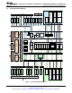
F28M36P63C, F28M36P53C, F28M36H53C, F28M36H53B, F28M36H33C, F28M36H33B www.ti.com SPRS825C – OCTOBER 2012 – REVISED FEBRUARY 2014 4 Terminal Description 4.1 Terminal Assignments Figure 4-1 illustrates the ball locations for the 289-ball ZWT new fine pitch ball grid array package and is used in conjunction with Figure 4-2, Figure 4-3, Figure 4-4, and Figure 4-5 to locate signal names and ball grid numbers.
F28M36P63C, F28M36P53C, F28M36H53C, F28M36H53B, F28M36H33C, F28M36H33B SPRS825C – OCTOBER 2012 – REVISED FEBRUARY 2014 www.ti.com Figure 4-2 through Figure 4-5 show the terminal assignments on the 289-ball ZWT package in four quadrants (A, B, C, and D). See Table 4-1, Terminal Functions, for the complete multiplexed signal names.
F28M36P63C, F28M36P53C, F28M36H53C, F28M36H53B, F28M36H33C, F28M36H33B www.ti.
F28M36P63C, F28M36P53C, F28M36H53C, F28M36H53B, F28M36H33C, F28M36H33B SPRS825C – OCTOBER 2012 – REVISED FEBRUARY 2014 10 11 12 13 J VSS VSS VSS VDDIO J H VSS VSS VSS VDDIO G VDDIO VDDIO VDDIO VDDIO 16 17 18 19 VSS PN1_ GPIO97 PN2_ GPIO98 X1 J H PJ7_ PN5_ GPIO63/ GPIO101 XCLKIN VSSOSC VSSOSC H G PP1_ PP0_ GPIO105 GPIO104 PN3_ GPIO99 X2 G F PD0_ GPIO16 PD1_ GPIO17 F E VSS PF1_ GPIO33 PP3_ VREG12EN GPIO107 VDDIO PF7_ GPIO39 PG4_ GPIO44 10 11 12 13 14 15
F28M36P63C, F28M36P53C, F28M36H53C, F28M36H53B, F28M36H33C, F28M36H33B www.ti.
F28M36P63C, F28M36P53C, F28M36H53C, F28M36H53B, F28M36H33C, F28M36H33B SPRS825C – OCTOBER 2012 – REVISED FEBRUARY 2014 4.2 www.ti.com Terminal Functions Table 4-1 describes the signals. Table 4-1. Terminal Functions(1) TERMINAL ZWT BALL NO. NAME I/O/Z(2) DESCRIPTION PU or PD(3) OUTPUT BUFFER STRENGTH ADC 1 Reference Inputs, Analog Comparator Inputs, DAC Inputs, AIO Group 1 ADC1VREFHI A12 I ADC1 External High Reference – used only when in ADC external reference mode.
F28M36P63C, F28M36P53C, F28M36H53C, F28M36H53B, F28M36H33C, F28M36H33B www.ti.com SPRS825C – OCTOBER 2012 – REVISED FEBRUARY 2014 Table 4-1. Terminal Functions(1) (continued) TERMINAL NAME ZWT BALL NO.
F28M36P63C, F28M36P53C, F28M36H53C, F28M36H53B, F28M36H33C, F28M36H33B SPRS825C – OCTOBER 2012 – REVISED FEBRUARY 2014 www.ti.com Table 4-1. Terminal Functions(1) (continued) TERMINAL NAME ZWT BALL NO.
F28M36P63C, F28M36P53C, F28M36H53C, F28M36H53B, F28M36H33C, F28M36H33B www.ti.com SPRS825C – OCTOBER 2012 – REVISED FEBRUARY 2014 Table 4-1. Terminal Functions(1) (continued) TERMINAL NAME ZWT BALL NO. I/O/Z(2) PG5_GPIO45 I/O/Z M_USB0DP Analog DESCRIPTION M_MIITXEN O EMAC MII transmit enable M_EPI0S40(5) I/O EPI-0 signal 40 PG6_GPIO46 I/O/Z W13 M_USB0ID Analog M_MIITXCK I M_EPI0S41(5) I/O PG7_GPIO47 I/O/Z M_MIITXER General-purpose input/output 46.
F28M36P63C, F28M36P53C, F28M36H53C, F28M36H53B, F28M36H33C, F28M36H33B SPRS825C – OCTOBER 2012 – REVISED FEBRUARY 2014 www.ti.com Table 4-1. Terminal Functions(1) (continued) TERMINAL NAME ZWT BALL NO.
F28M36P63C, F28M36P53C, F28M36H53C, F28M36H53B, F28M36H33C, F28M36H33B www.ti.com SPRS825C – OCTOBER 2012 – REVISED FEBRUARY 2014 Table 4-1. Terminal Functions(1) (continued) TERMINAL NAME ZWT BALL NO.
F28M36P63C, F28M36P53C, F28M36H53C, F28M36H53B, F28M36H33C, F28M36H33B SPRS825C – OCTOBER 2012 – REVISED FEBRUARY 2014 www.ti.com Table 4-1. Terminal Functions(1) (continued) TERMINAL NAME ZWT BALL NO.
F28M36P63C, F28M36P53C, F28M36H53C, F28M36H53B, F28M36H33C, F28M36H33B www.ti.com SPRS825C – OCTOBER 2012 – REVISED FEBRUARY 2014 Table 4-1. Terminal Functions(1) (continued) TERMINAL NAME PR5_GPIO125 C_EPWM7B PR6_GPIO126 C_EPWM8A PR7_GPIO127 C_EPWM8B PS0_GPIO128 C_EPWM9A PS1_GPIO129 C_EPWM9B PS2_GPIO130 C_EPWM10A PS3_GPIO131 C_EPWM10B PS4_GPIO132 C_EPWM11A PS5_GPIO133 C_EPWM11B PS6_GPIO134 C_EPWM12A PS7_GPIO135 C_EPWM12B ZWT BALL NO.
F28M36P63C, F28M36P53C, F28M36H53C, F28M36H53B, F28M36H33C, F28M36H33B SPRS825C – OCTOBER 2012 – REVISED FEBRUARY 2014 www.ti.com Table 4-1. Terminal Functions(1) (continued) TERMINAL NAME ZWT BALL NO. I/O/Z(2) DESCRIPTION PU or PD(3) OUTPUT BUFFER STRENGTH I/OD Digital Subsystem Reset (in) and Watchdog/Power-on Reset (out). In most applications, TI recommends that the XRS pin be tied with the ARS pin.
F28M36P63C, F28M36P53C, F28M36H53C, F28M36H53B, F28M36H33C, F28M36H33B www.ti.com SPRS825C – OCTOBER 2012 – REVISED FEBRUARY 2014 Table 4-1. Terminal Functions(1) (continued) TERMINAL NAME ZWT BALL NO. I/O/Z(2) DESCRIPTION PU or PD(3) OUTPUT BUFFER STRENGTH Clocks X1 X2 J19 G19 I External oscillator input or on-chip crystaloscillator input. To use the on-chip oscillator, a quartz crystal or a ceramic resonator must be connected across X1 and X2. See Figure 3-7.
F28M36P63C, F28M36P53C, F28M36H53C, F28M36H53B, F28M36H33C, F28M36H33B SPRS825C – OCTOBER 2012 – REVISED FEBRUARY 2014 www.ti.com Table 4-1. Terminal Functions(1) (continued) TERMINAL PU or PD(3) OUTPUT BUFFER STRENGTH ZWT BALL NO. I/O/Z(2) TDI K19 I JTAG test data input (TDI) with internal pullup. TDI is clocked into the selected register (instruction or data) on a rising edge of TCK. TDO T19 O JTAG scan out, test data output (TDO).
F28M36P63C, F28M36P53C, F28M36H53C, F28M36H53B, F28M36H33C, F28M36H33B www.ti.com SPRS825C – OCTOBER 2012 – REVISED FEBRUARY 2014 Table 4-1. Terminal Functions(1) (continued) TERMINAL NAME ZWT BALL NO.
F28M36P63C, F28M36P53C, F28M36H53C, F28M36H53B, F28M36H33C, F28M36H33B SPRS825C – OCTOBER 2012 – REVISED FEBRUARY 2014 www.ti.com Table 4-1. Terminal Functions(1) (continued) TERMINAL NAME ZWT BALL NO.
F28M36P63C, F28M36P53C, F28M36H53C, F28M36H53B, F28M36H33C, F28M36H33B www.ti.com SPRS825C – OCTOBER 2012 – REVISED FEBRUARY 2014 Table 4-1. Terminal Functions(1) (continued) TERMINAL NAME ZWT BALL NO. I/O/Z(2) DESCRIPTION PU or PD(3) OUTPUT BUFFER STRENGTH Digital Logic Power Pins (Master and Control Subsystems) VDD12 M7 VDD12 M13 VDD12 N7 VDD12 N12 VDD12 N13 VDD12 T10 VDD12 T11 VDD12 T12 VSS A1 VSS A2 VSS A18 VSS A19 1.
F28M36P63C, F28M36P53C, F28M36H53C, F28M36H53B, F28M36H33C, F28M36H33B SPRS825C – OCTOBER 2012 – REVISED FEBRUARY 2014 www.ti.com Table 4-1. Terminal Functions(1) (continued) TERMINAL NAME ZWT BALL NO.
F28M36P63C, F28M36P53C, F28M36H53C, F28M36H53B, F28M36H33C, F28M36H33B www.ti.com SPRS825C – OCTOBER 2012 – REVISED FEBRUARY 2014 5 Device Operating Conditions Absolute Maximum Ratings (1) 5.1 (2) Supply voltage range, VDDIO (I/O and Flash) with respect to VSS –0.3 V to 4.6 V Supply voltage range, VDD18 with respect to VSS –0.3 V to 2.5 V Supply voltage range, VDD12 with respect to VSS –0.3 V to 1.5 V Analog voltage range, VDDA with respect to VSSA –0.3 V to 4.
F28M36P63C, F28M36P53C, F28M36H53C, F28M36H53B, F28M36H33C, F28M36H33B SPRS825C – OCTOBER 2012 – REVISED FEBRUARY 2014 5.3 www.ti.com Recommended Operating Conditions MIN NOM MAX UNIT Device supply voltage, I/O, VDDIO (1) 2.97 3.3 3.63 V Device supply voltage, Analog Subsystem, VDD18 (when internal VREG is disabled and 1.8 V is supplied externally) 1.71 1.8 1.995 Device supply voltage, Master and Control Subsystems, VDD12 (when internal VREG is disabled and 1.2 V is supplied externally) 1.
F28M36P63C, F28M36P53C, F28M36H53C, F28M36H53B, F28M36H33C, F28M36H33B www.ti.com 5.4 SPRS825C – OCTOBER 2012 – REVISED FEBRUARY 2014 Electrical Characteristics over recommended operating conditions (unless otherwise noted) PARAMETER VOH High-level output voltage VOL Low-level output voltage TEST CONDITIONS IOH = IOH MAX VDDIO * 0.8 IOH = 50 μA VDDIO – 0.2 IIH Input current (low level) Input current (high level) Pin with pullup enabled VDDIO = 3.3 V, VIN = 0 V MAX UNIT V VDDIO * 0.
F28M36P63C, F28M36P53C, F28M36H53C, F28M36H53B, F28M36H33C, F28M36H33B SPRS825C – OCTOBER 2012 – REVISED FEBRUARY 2014 www.ti.com 6 Electrical Specifications 6.1 Current Consumption Table 6-1.
F28M36P63C, F28M36P53C, F28M36H53C, F28M36H53B, F28M36H33C, F28M36H33B www.ti.com SPRS825C – OCTOBER 2012 – REVISED FEBRUARY 2014 Table 6-1. Current Consumption at 150-MHz C28x SYSCLKOUT and 75-MHz M3SSCLK (continued) VREG ENABLED TEST CONDITIONS (1) MODE SLEEP IDLE SLEEP STANDBY DEEP SLEEP STANDBY • PLL is on. • Cortex-M3 CPU is not executing. • M3SSCLK is on. • C28CLKIN is on. • C28x CPU is not executing. • C28CPUCLK is off. • C28SYSCLK is on. • PLL is on.
F28M36P63C, F28M36P53C, F28M36H53C, F28M36H53B, F28M36H33C, F28M36H33B SPRS825C – OCTOBER 2012 – REVISED FEBRUARY 2014 www.ti.com Table 6-2.
F28M36P63C, F28M36P53C, F28M36H53C, F28M36H53B, F28M36H33C, F28M36H33B www.ti.com SPRS825C – OCTOBER 2012 – REVISED FEBRUARY 2014 Table 6-2. Current Consumption at 125-MHz C28x SYSCLKOUT and 125-MHz M3SSCLK (continued) VREG ENABLED TEST CONDITIONS (1) MODE SLEEP IDLE SLEEP STANDBY DEEP SLEEP STANDBY • PLL is on. • Cortex-M3 CPU is not executing. • M3SSCLK is on. • C28CLKIN is on. • C28x CPU is not executing. • C28CPUCLK is off. • C28SYSCLK is on. • PLL is on.
F28M36P63C, F28M36P53C, F28M36H53C, F28M36H53B, F28M36H33C, F28M36H33B SPRS825C – OCTOBER 2012 – REVISED FEBRUARY 2014 6.2 www.ti.com Thermal Design Considerations Based on the end-application design and operational profile, the IDD12, IDD18, and IDDIO currents could vary. Systems that exceed the recommended maximum power dissipation in the end product may require additional thermal enhancements. Ambient temperature (TA) varies with the end application and product design.
F28M36P63C, F28M36P53C, F28M36H53C, F28M36H53B, F28M36H33C, F28M36H33B www.ti.com 6.3 SPRS825C – OCTOBER 2012 – REVISED FEBRUARY 2014 Timing Parameter Symbology Timing parameter symbols used are created in accordance with JEDEC Standard 100. To shorten the symbols, some of the pin names and other related terminology have been abbreviated as follows: 6.3.
F28M36P63C, F28M36P53C, F28M36H53C, F28M36H53B, F28M36H33C, F28M36H33B SPRS825C – OCTOBER 2012 – REVISED FEBRUARY 2014 6.4 www.ti.com Clock Frequencies, Requirements, and Characteristics This section provides the frequencies and timing requirements of the input clocks; PLL lock times; frequencies of the internal clocks; and the frequency and switching characteristics of the output clock. 6.4.
F28M36P63C, F28M36P53C, F28M36H53C, F28M36H53B, F28M36H33C, F28M36H33B www.ti.com SPRS825C – OCTOBER 2012 – REVISED FEBRUARY 2014 Table 6-7.
F28M36P63C, F28M36P53C, F28M36H53C, F28M36H53B, F28M36H33C, F28M36H33B SPRS825C – OCTOBER 2012 – REVISED FEBRUARY 2014 6.4.3 www.ti.com Output Clock Frequency and Switching Characteristics Table 6-11 provides the frequency of the output clock from the F28M36x devices. Table 6-12 shows the switching characteristics of the output clock from the F28M36x devices, XCLKOUT. Table 6-11. Output Clock Frequency f(XCO) Frequency, XCLKOUT MIN MAX UNIT 2 37.5 MHz Table 6-12.
F28M36P63C, F28M36P53C, F28M36H53C, F28M36H53B, F28M36H33C, F28M36H33B www.ti.com 6.5 SPRS825C – OCTOBER 2012 – REVISED FEBRUARY 2014 Power Sequencing There is no power sequencing requirement needed to ensure the device is in the proper state after reset or to prevent the I/Os from glitching during power up and power down. (All I/Os, except for GPIO199, are glitch-free during power up and power down.) No voltage larger than a diode drop (0.
F28M36P63C, F28M36P53C, F28M36H53C, F28M36H53B, F28M36H33C, F28M36H33B SPRS825C – OCTOBER 2012 – REVISED FEBRUARY 2014 www.ti.com Table 6-13. Reset (XRS) Timing Requirements MIN th(boot-mode) Hold time for boot-mode pins tw(RSL2) Pulse duration, XRS low on warm reset MAX UNIT 14000tc(M3C) cycles 32tc(OCK) cycles Table 6-14.
F28M36P63C, F28M36P53C, F28M36H53C, F28M36H53B, F28M36H33C, F28M36H33B www.ti.com 6.5.1 SPRS825C – OCTOBER 2012 – REVISED FEBRUARY 2014 Changing the Frequency of the Main PLL Figure 6-4 shows how to change the frequency of the Main PLL. The three steps are described below: 1. The PLL must first be placed in bypass mode (by writing to the SYSPLLCTL register) before any changes are made to the SPLLIMULT and SPLLFMULT fields of the SYSPLLMULT Register.
F28M36P63C, F28M36P53C, F28M36H53C, F28M36H53B, F28M36H33C, F28M36H33B SPRS825C – OCTOBER 2012 – REVISED FEBRUARY 2014 6.5.2 www.ti.com Power Management and Supervisory Circuit Solutions Table 6-15 lists the power management and supervisory circuit solutions for F28M36x devices. LDO selection depends on the total power consumed in the end application. Go to www.ti.
F28M36P63C, F28M36P53C, F28M36H53C, F28M36H53B, F28M36H33C, F28M36H33B www.ti.com 6.6 SPRS825C – OCTOBER 2012 – REVISED FEBRUARY 2014 Flash Timing – Master Subsystem Table 6-16.
F28M36P63C, F28M36P53C, F28M36H53C, F28M36H53B, F28M36H33C, F28M36H33B SPRS825C – OCTOBER 2012 – REVISED FEBRUARY 2014 www.ti.com Table 6-20. Master Subsystem – Flash Parameters at 125 MHz (1) (2) PARAMETER Program Time Erase Time (1) (2) (3) (3) TEST CONDITIONS MIN TYP MAX UNIT 128 bits 240 μs 32K Sector 500 ms 128K Sector 2000 ms 32K Sector 50 ms 128K Sector 50 ms The on-chip flash memory is in an erased state when the device is shipped from TI.
F28M36P63C, F28M36P53C, F28M36H53C, F28M36H53B, F28M36H33C, F28M36H33B www.ti.com SPRS825C – OCTOBER 2012 – REVISED FEBRUARY 2014 Table 6-23. Master Subsystem – Minimum Required Flash/OTP Wait-States at Different Frequencies SYSCLKOUT (MHz) SYSCLKOUT (ns) WAIT-STATE 125 8 3 120 8.33 2 110 9.1 2 100 10 2 90 11.11 2 80 12.5 1 70 14.29 1 60 16.67 1 50 20 1 40 25 0 30 33.
F28M36P63C, F28M36P53C, F28M36H53C, F28M36H53B, F28M36H33C, F28M36H33B SPRS825C – OCTOBER 2012 – REVISED FEBRUARY 2014 6.7 www.ti.com Flash Timing – Control Subsystem Table 6-24.
F28M36P63C, F28M36P53C, F28M36H53C, F28M36H53B, F28M36H33C, F28M36H33B www.ti.com SPRS825C – OCTOBER 2012 – REVISED FEBRUARY 2014 Table 6-28.
F28M36P63C, F28M36P53C, F28M36H53C, F28M36H53B, F28M36H33C, F28M36H33B SPRS825C – OCTOBER 2012 – REVISED FEBRUARY 2014 www.ti.com Table 6-31. Control Subsystem – Minimum Required Flash/OTP Wait-States at Different Frequencies SYSCLKOUT (MHz) SYSCLKOUT (ns) WAIT-STATE 150 6.7 3 140 7.14 3 130 7.7 3 120 8.33 2 110 9.1 2 100 10 2 90 11.11 2 80 12.5 1 70 14.29 1 60 16.67 1 50 20 1 40 25 0 30 33.
F28M36P63C, F28M36P53C, F28M36H53C, F28M36H53B, F28M36H33C, F28M36H33B www.ti.com 6.8 6.8.1 SPRS825C – OCTOBER 2012 – REVISED FEBRUARY 2014 GPIO Electrical Data and Timing GPIO - Output Timing Table 6-32.
F28M36P63C, F28M36P53C, F28M36H53C, F28M36H53B, F28M36H33C, F28M36H33B SPRS825C – OCTOBER 2012 – REVISED FEBRUARY 2014 6.8.2 www.ti.com GPIO - Input Timing Table 6-33.
F28M36P63C, F28M36P53C, F28M36H53C, F28M36H53B, F28M36H33C, F28M36H33B www.ti.com 6.8.3 SPRS825C – OCTOBER 2012 – REVISED FEBRUARY 2014 Sampling Window Width for Input Signals The following section summarizes the sampling window width for input signals for various input qualifier configurations. Sampling frequency denotes how often a signal is sampled with respect to SYSCLKOUT.
F28M36P63C, F28M36P53C, F28M36H53C, F28M36H53B, F28M36H33C, F28M36H33B SPRS825C – OCTOBER 2012 – REVISED FEBRUARY 2014 6.8.4 www.ti.com Low-Power Mode Wakeup Timing Table 6-34 shows the timing requirements, Table 6-35 shows the switching characteristics, and Figure 6-8 shows the timing diagram for IDLE mode. Table 6-34.
F28M36P63C, F28M36P53C, F28M36H53C, F28M36H53B, F28M36H33C, F28M36H33B www.ti.com SPRS825C – OCTOBER 2012 – REVISED FEBRUARY 2014 Table 6-36. STANDBY Mode Timing Requirements MIN tw(WAKE-INT) (1) Pulse duration, external wake-up signal Without input qualification With input qualification (1) MAX 3tc(OSCCLK) UNIT cycles (2 + QUALSTDBY) * tc(OSCCLK) QUALSTDBY is a 6-bit field in the LPMCR0 register. Table 6-37.
F28M36P63C, F28M36P53C, F28M36H53C, F28M36H53B, F28M36H33C, F28M36H33B SPRS825C – OCTOBER 2012 – REVISED FEBRUARY 2014 (A) www.ti.com (C) (B) STANDBY Device Status (E) (D) STANDBY (F) Normal Execution Flushing Pipeline (G) Wake-up Signal tw(WAKE-INT) td(WAKE-STBY) X1/X2 or X1 or XCLKIN XCLKOUT td(IDLE-XCOL) A. B. C. D. E. F. G. IDLE instruction is executed to put the device into STANDBY mode. The PLL block responds to the STANDBY signal.
F28M36P63C, F28M36P53C, F28M36H53C, F28M36H53B, F28M36H33C, F28M36H33B www.ti.com SPRS825C – OCTOBER 2012 – REVISED FEBRUARY 2014 Table 6-38. HALT Mode Timing Requirements MIN tw(WAKE-GPIO) Pulse duration, GPIO wake-up signal tw(WAKE-XRS) Pulse duration, XRS wakeup signal (1) MAX UNIT (1) cycles toscst + 8tc(OSCCLK) cycles toscst + 2tc(OSCCLK) See Table 6-14 for an explanation of toscst. Table 6-39.
F28M36P63C, F28M36P53C, F28M36H53C, F28M36H53B, F28M36H33C, F28M36H33B SPRS825C – OCTOBER 2012 – REVISED FEBRUARY 2014 (A) www.ti.com (C) Device Status (D) HALT Flushing Pipeline (G) (E) (B) (F) HALT PLL Lock-up Time Wake-up Latency Normal Execution (H) GPIOn td(WAKE-HALT) tw(WAKE-GPIO) tp X1/X2 or XCLKIN Oscillator Start-up Time XCLKOUT td(IDLE−XCOL) A. B. C. D. E. F. G. H. IDLE instruction is executed to put the device into HALT mode. The PLL block responds to the HALT signal.
F28M36P63C, F28M36P53C, F28M36H53C, F28M36H53B, F28M36H33C, F28M36H33B www.ti.com 6.9 SPRS825C – OCTOBER 2012 – REVISED FEBRUARY 2014 External Interrupt Electrical Data and Timing Table 6-40. External Interrupt Timing Requirements (1) MIN tw(INT) (1) (2) (2) Pulse duration, INT input low/high MAX UNIT Synchronous 1tc(SCO) cycles With qualifier 1tc(SCO) + tw(IQSW) cycles For an explanation of the input qualifier parameters, see Table 6-33.
F28M36P63C, F28M36P53C, F28M36H53C, F28M36H53B, F28M36H33C, F28M36H33B SPRS825C – OCTOBER 2012 – REVISED FEBRUARY 2014 www.ti.com 7 Peripheral Information and Timings 7.1 Analog and Shared Peripherals Concerto Shared Peripherals are accessible from both the Master Subsystem and the Control Subsystem. The Analog Shared Peripherals include two 12-bit ADCs (Analog-to-Digital Converters), and six Comparator + DAC (10-bit) modules.
F28M36P63C, F28M36P53C, F28M36H53C, F28M36H53B, F28M36H33C, F28M36H33B www.ti.
F28M36P63C, F28M36P53C, F28M36H53C, F28M36H53B, F28M36H33C, F28M36H33B SPRS825C – OCTOBER 2012 – REVISED FEBRUARY 2014 7.1.1.2 www.ti.com Start-of-Conversion Triggers There are eight external SOC triggers that go to each of the two ADC modules (from the Control Subsystem). In addition to the eight external SOC triggers, there are also two internal SOC triggers derived from EOC interrupts inside each ADC module (ADCINT1 and ADCINT2).
F28M36P63C, F28M36P53C, F28M36H53C, F28M36H53B, F28M36H33C, F28M36H33B www.ti.com 7.1.1.5 SPRS825C – OCTOBER 2012 – REVISED FEBRUARY 2014 ADC Electrical Data and Timing Table 7-1. ADC Electrical Characteristics over recommended operating conditions (unless otherwise noted) PARAMETER MIN TYP MAX UNIT MHz DC SPECIFICATIONS Resolution 12 Bits ADC clock 2 37.5 Sample Window 7 64 ADC Clocks –4 4 LSB ACCURACY INL (Integral nonlinearity) DNL (Differential nonlinearity) Offset error 1.
F28M36P63C, F28M36P53C, F28M36H53C, F28M36H53B, F28M36H33C, F28M36H33B SPRS825C – OCTOBER 2012 – REVISED FEBRUARY 2014 www.ti.com Typical ADC Total Error 80 70 Total Error (LSBs) 60 50 40 30 20 10 0 -40 -35 -30 -25 -20 -15 -10 -5 0 5 10 15 20 25 30 35 40 45 50 55 60 65 70 75 80 85 90 95 100 105 110 115 120 125 Temperature (°C) A. B. C. Gain error contribution is based on sampling of full-scale voltage using internal reference mode. Periodic ADC offset re-cal is assumed.
F28M36P63C, F28M36P53C, F28M36H53C, F28M36H53B, F28M36H33C, F28M36H33B www.ti.
F28M36P63C, F28M36P53C, F28M36H53C, F28M36H53B, F28M36H33C, F28M36H33B SPRS825C – OCTOBER 2012 – REVISED FEBRUARY 2014 7.1.2.1 www.ti.com On-Chip Comparator and DAC Electrical Data and Timing Table 7-3.
F28M36P63C, F28M36P53C, F28M36H53C, F28M36H53B, F28M36H33C, F28M36H33B www.ti.com 7.1.3 SPRS825C – OCTOBER 2012 – REVISED FEBRUARY 2014 Interprocessor Communications Figure 7-6 shows the internal structure of the IPC peripheral used to synchronize program execution and exchange of data between the Cortex-M3 and the C28x CPU. IPC can be used by itself when synchronizing program execution or it can be used in conjunction with Message RAMs when coordinating data transfers between processors.
F28M36P63C, F28M36P53C, F28M36H53C, F28M36H53B, F28M36H33C, F28M36H33B SPRS825C – OCTOBER 2012 – REVISED FEBRUARY 2014 www.ti.com INTRS M3 CPU WRDATA (31:0) SET(31:0) CTOM IPC INT (3:0) NVIC STS(3:0) STS(31:0) FLG(31:0) ACK(31:0) RDDATA (31:0) M3 SYSTEM BUS M3 32 MTOC IPC CHANNELS 3 4 MTOC_CH0 MTOC_CH1 MTOC_CH2 MTOC_CH29 MTOC_CH30 MTOC_CH31 ACK FLG STS SET MTOCIPCSET REG MTOCIPCFLG REG MTOCIPCSTS REG ... FLG REG 31 ... 0 STS REG 31 ...
F28M36P63C, F28M36P53C, F28M36H53C, F28M36H53B, F28M36H33C, F28M36H33B www.ti.com 7.1.4 SPRS825C – OCTOBER 2012 – REVISED FEBRUARY 2014 External Peripheral Interface The EPI provides a high-speed parallel bus for interfacing external peripherals and memory. EPI is accessible from both the Master Subsystem and the Control Subsystem. EPI has several modes of operation to enable glueless connectivity to most types of external devices.
F28M36P63C, F28M36P53C, F28M36H53C, F28M36H53B, F28M36H33C, F28M36H33B SPRS825C – OCTOBER 2012 – REVISED FEBRUARY 2014 www.ti.
F28M36P63C, F28M36P53C, F28M36H53C, F28M36H53B, F28M36H33C, F28M36H33B www.ti.com SPRS825C – OCTOBER 2012 – REVISED FEBRUARY 2014 EPI can directly interrupt the Cortex-M3 CPU, the Cortex-M3 uDMA, and the C28x CPU (but not the C28x DMA) via the EPI interrupt. Typically, EPI interrupts are used to prompt the CPU or DMA to move data to and from EPI. There are four EPI Interrupt registers that control various facets of interrupt generation, clearing, and masking.
F28M36P63C, F28M36P53C, F28M36H53C, F28M36H53B, F28M36H33C, F28M36H33B SPRS825C – OCTOBER 2012 – REVISED FEBRUARY 2014 EPI CONFIG REG www.ti.
F28M36P63C, F28M36P53C, F28M36H53C, F28M36H53B, F28M36H33C, F28M36H33B www.ti.com SPRS825C – OCTOBER 2012 – REVISED FEBRUARY 2014 Table 7-4.
F28M36P63C, F28M36P53C, F28M36H53C, F28M36H53B, F28M36H33C, F28M36H33B SPRS825C – OCTOBER 2012 – REVISED FEBRUARY 2014 7.1.4.2 www.ti.com EPI SDRAM Mode The EPI SDRAM Mode combines high performance, low cost, and low pin utilization to access up to 512 megabits (Mb) of external memory.
F28M36P63C, F28M36P53C, F28M36H53C, F28M36H53B, F28M36H33C, F28M36H33B www.ti.com SPRS825C – OCTOBER 2012 – REVISED FEBRUARY 2014 Table 7-5.
F28M36P63C, F28M36P53C, F28M36H53C, F28M36H53B, F28M36H33C, F28M36H33B SPRS825C – OCTOBER 2012 – REVISED FEBRUARY 2014 7.1.4.3 www.ti.com EPI Host Bus Mode There are two versions of the EPI Host Bus Mode: an 8-bit version (HB-8) and a 16-bit version (HB-16). Section 7.1.4.3.1 discusses the EPI 8-Bit Host Bus Mode. Section 7.1.4.3.2 discusses the EPI 16-Bit Host Bus Mode. 7.1.4.3.
F28M36P63C, F28M36P53C, F28M36H53C, F28M36H53B, F28M36H33C, F28M36H33B www.ti.com SPRS825C – OCTOBER 2012 – REVISED FEBRUARY 2014 Table 7-6.
F28M36P63C, F28M36P53C, F28M36H53C, F28M36H53B, F28M36H33C, F28M36H33B SPRS825C – OCTOBER 2012 – REVISED FEBRUARY 2014 www.ti.com 7.1.4.3.1.2 HB-8 Non-Muxed Address/Data Mode The HB-8 Non-Muxed Mode uses dedicated pins for address and data signals. For this reason, the NonMuxed Mode has reduced address reach as compared to the Muxed Mode. The HB-8 Non-Muxed Mode is selected with the MODE field of the HB-8 Configuration Register.
F28M36P63C, F28M36P53C, F28M36H53C, F28M36H53B, F28M36H33C, F28M36H33B www.ti.com SPRS825C – OCTOBER 2012 – REVISED FEBRUARY 2014 Table 7-7.
F28M36P63C, F28M36P53C, F28M36H53C, F28M36H53B, F28M36H33C, F28M36H33B SPRS825C – OCTOBER 2012 – REVISED FEBRUARY 2014 www.ti.com Table 7-8.
F28M36P63C, F28M36P53C, F28M36H53C, F28M36H53B, F28M36H33C, F28M36H33B www.ti.com SPRS825C – OCTOBER 2012 – REVISED FEBRUARY 2014 7.1.4.3.2 EPI 16-Bit Host Bus (HB-16) Mode The 16-Bit Host Bus (HB-16) Mode uses fewer address pins than the 8-Bit Host Bus (HB-8) Mode; hence, more pins are available for data. The HB-16 Mode is also slower than the General-Purpose Mode in order to accommodate older logic. The HB-16 Mode is selected with the MODE field of EPI Configuration Register.
F28M36P63C, F28M36P53C, F28M36H53C, F28M36H53B, F28M36H33C, F28M36H33B SPRS825C – OCTOBER 2012 – REVISED FEBRUARY 2014 www.ti.com 7.1.4.3.2.1 HB-16 Muxed Address/Data Mode The HB-16 Muxed Mode multiplexes address signals with low-order data signals. For this reason, the Muxed Mode allows for a larger address space as compared to the Non-Muxed Mode. The HB-16 Muxed Mode is selected with the MODE field of the HB-16 Configuration Register.
F28M36P63C, F28M36P53C, F28M36H53C, F28M36H53B, F28M36H33C, F28M36H33B www.ti.com SPRS825C – OCTOBER 2012 – REVISED FEBRUARY 2014 Table 7-9.
F28M36P63C, F28M36P53C, F28M36H53C, F28M36H53B, F28M36H33C, F28M36H33B SPRS825C – OCTOBER 2012 – REVISED FEBRUARY 2014 www.ti.com Table 7-10.
F28M36P63C, F28M36P53C, F28M36H53C, F28M36H53B, F28M36H33C, F28M36H33B www.ti.com SPRS825C – OCTOBER 2012 – REVISED FEBRUARY 2014 Table 7-11.
F28M36P63C, F28M36P53C, F28M36H53C, F28M36H53B, F28M36H33C, F28M36H33B SPRS825C – OCTOBER 2012 – REVISED FEBRUARY 2014 www.ti.com Table 7-12.
F28M36P63C, F28M36P53C, F28M36H53C, F28M36H53B, F28M36H33C, F28M36H33B www.ti.com SPRS825C – OCTOBER 2012 – REVISED FEBRUARY 2014 Table 7-13.
F28M36P63C, F28M36P53C, F28M36H53C, F28M36H53B, F28M36H33C, F28M36H33B SPRS825C – OCTOBER 2012 – REVISED FEBRUARY 2014 www.ti.com Table 7-14.
F28M36P63C, F28M36P53C, F28M36H53C, F28M36H53B, F28M36H33C, F28M36H33B www.ti.com SPRS825C – OCTOBER 2012 – REVISED FEBRUARY 2014 7.1.4.3.2.3 HB-16 FIFO Mode The HB-16 FIFO Mode uses 16 bits of data, removes ALE and address pins, and optionally adds external FIFO Full/Empty flag inputs. This scheme is used by many devices, such as radios, communication devices (including USB2 devices), and some FPGA configuration (FIFO throughblock RAM).
F28M36P63C, F28M36P53C, F28M36H53C, F28M36H53B, F28M36H33C, F28M36H33B SPRS825C – OCTOBER 2012 – REVISED FEBRUARY 2014 www.ti.com Table 7-15.
F28M36P63C, F28M36P53C, F28M36H53C, F28M36H53B, F28M36H33C, F28M36H33B www.ti.com SPRS825C – OCTOBER 2012 – REVISED FEBRUARY 2014 Table 7-17. EPI SDRAM Interface Switching Characteristics Over Recommended Operating Conditions (Unless Otherwise Noted) (see Figure 7-12, Figure 7-13, and Figure 7-14) NO.
F28M36P63C, F28M36P53C, F28M36H53C, F28M36H53B, F28M36H33C, F28M36H33B SPRS825C – OCTOBER 2012 – REVISED FEBRUARY 2014 www.ti.com CLK (EPI0S31) CKE (EPI0S30) E4 E5 E6 CS (EPI0S29) WE (EPI0S28) RAS (EPI0S19) CAS (EPI0S18) DQMH, DQML (EPI0S [17:16]) AD [15:0] (EPI0S [15:0]) Row Activate Column-1 NOP NOP Data 0 Data 1 ... Data n Burst Term Write AD [15:0] driven out AD [15:0] driven out Figure 7-14.
F28M36P63C, F28M36P53C, F28M36H53C, F28M36H53B, F28M36H33C, F28M36H33B www.ti.com SPRS825C – OCTOBER 2012 – REVISED FEBRUARY 2014 Table 7-18. EPI Host-Bus 8 and Host-Bus 16 Interface Switching Characteristics Over Recommended Operating Conditions (Unless Otherwise Noted) (see Figure 7-15, Figure 7-16, Figure 7-17, and Figure 7-18) NO.
F28M36P63C, F28M36P53C, F28M36H53C, F28M36H53B, F28M36H33C, F28M36H33B SPRS825C – OCTOBER 2012 – REVISED FEBRUARY 2014 www.ti.com E22 ALE (EPI0S30) E18 E23 CS (EPI0S30) E18 E19 E20 WR (EPI0S29) E24 RD/OE (EPI0S28) BSEL0/BSEL1 (A) Address E16 E17 Data Data A. BSEL0 and BSEL1 are available in Host-Bus 16 mode only. Figure 7-16.
F28M36P63C, F28M36P53C, F28M36H53C, F28M36H53B, F28M36H33C, F28M36H33B www.ti.com SPRS825C – OCTOBER 2012 – REVISED FEBRUARY 2014 Table 7-20. EPI General-Purpose Interface Switching Characteristics Over Recommended Operating Conditions (Unless Otherwise Noted) (see Figure 7-19) NO.
F28M36P63C, F28M36P53C, F28M36H53C, F28M36H53B, F28M36H33C, F28M36H33B SPRS825C – OCTOBER 2012 – REVISED FEBRUARY 2014 7.2 www.ti.com Master Subsystem Peripherals Master Subsystem peripherals are located on the APB Bus and AHB Bus, and are accessible from the Cortex-M3 CPU/µDMA. The AHB peripherals include EPI, USB, and two CAN modules. The APB peripherals include EMAC, two I2Cs, five UARTs, four SSIs, four GPTIMERs, two WDOGs, NMI WDOG, and a µCRC module (Cyclic Redundancy Check).
F28M36P63C, F28M36P53C, F28M36H53C, F28M36H53B, F28M36H33C, F28M36H33B www.ti.
F28M36P63C, F28M36P53C, F28M36H53C, F28M36H53B, F28M36H33C, F28M36H33B SPRS825C – OCTOBER 2012 – REVISED FEBRUARY 2014 7.2.1.2 www.ti.com Transmit FIFO The transmit FIFO is a 16-bit-wide, 8-location-deep, first-in, first-out memory buffer. The CPU writes data to the FIFO through the SSI Data (SSIDR) register, and data is stored in the FIFO until the data is read out by the transmission logic.
F28M36P63C, F28M36P53C, F28M36H53C, F28M36H53B, F28M36H33C, F28M36H33B www.ti.com 7.2.1.5 SPRS825C – OCTOBER 2012 – REVISED FEBRUARY 2014 Frame Formats Each data frame is between 4 bits and 16 bits long, depending on the size of data programmed, and is transmitted starting with the MSB.
F28M36P63C, F28M36P53C, F28M36H53C, F28M36H53B, F28M36H33C, F28M36H33B SPRS825C – OCTOBER 2012 – REVISED FEBRUARY 2014 7.2.2 www.ti.com Universal Asynchronous Receiver/Transmitter This device has five UART modules. The CPU accesses data, control, and status information. The UART also supports µDMA transfers. Each UART performs functions of parallel-to-serial and serial-to-parallel conversions. Each of the five UART modules is similar in functionality to a 16C550 UART, but is not register-compatible.
F28M36P63C, F28M36P53C, F28M36H53C, F28M36H53B, F28M36H33C, F28M36H33B www.ti.
F28M36P63C, F28M36P53C, F28M36H53C, F28M36H53B, F28M36H33C, F28M36H33B SPRS825C – OCTOBER 2012 – REVISED FEBRUARY 2014 7.2.2.2 www.ti.com Transmit and Receive Logic The transmit logic performs parallel-to-serial conversion on the data read from the transmit FIFO. The control logic outputs the serial bit stream beginning with a start bit and followed by the data bits (LSB first), parity bit, and the stop bits according to the programmed configuration in the control registers.
F28M36P63C, F28M36P53C, F28M36H53C, F28M36H53B, F28M36H33C, F28M36H33B www.ti.com 7.2.2.
F28M36P63C, F28M36P53C, F28M36H53C, F28M36H53B, F28M36H33C, F28M36H33B SPRS825C – OCTOBER 2012 – REVISED FEBRUARY 2014 7.2.3 www.ti.com Cortex-M3 Inter-Integrated Circuit This device has two Cortex-M3 I2C peripherals. The Cortex-M3 I2C bus provides bidirectional data transfer through a two-wire design (a serial data line SDA and a serial clock line SCL), and interfaces to external I2C devices such as serial memory (RAMs and ROMs), networking devices, LCDs, tone generators, and so on.
F28M36P63C, F28M36P53C, F28M36H53C, F28M36H53B, F28M36H33C, F28M36H33B www.ti.
F28M36P63C, F28M36P53C, F28M36H53C, F28M36H53B, F28M36H33C, F28M36H33B SPRS825C – OCTOBER 2012 – REVISED FEBRUARY 2014 7.2.3.3 www.ti.com I2C Electrical Data and Timing Table 7-22.
F28M36P63C, F28M36P53C, F28M36H53C, F28M36H53B, F28M36H33C, F28M36H33B www.ti.com 7.2.4 SPRS825C – OCTOBER 2012 – REVISED FEBRUARY 2014 Cortex-M3 Controller Area Network This device has two Cortex-M3 CAN peripherals. CAN is a serial communications protocol that efficiently supports distributed real-time control with a high level of security. The CAN module supports bit rates up to 1 Mbit/s and is compliant with the CAN 2.0B protocol specification.
F28M36P63C, F28M36P53C, F28M36H53C, F28M36H53B, F28M36H33C, F28M36H33B SPRS825C – OCTOBER 2012 – REVISED FEBRUARY 2014 CANxIRQ M3 NVIC www.ti.com INTR M3 CPU M3 CLOCKS M3SSCLK M3CLKENBx REGISTER ACCESS CAN (M3) CANxCLK CANxTX MODULE INTERFACE PIN MESSAGE RAM GPIO_MUX1 REGISTERS AND MESSAGE OBJECT ACCESS (IFX) CAN CORE 32 MESSAGE OBJECTS MESSAGE RAM INTERFACE CANxRX MESSAGE HANDLER PIN Figure 7-24.
F28M36P63C, F28M36P53C, F28M36H53C, F28M36H53B, F28M36H33C, F28M36H33B www.ti.com 7.2.5 SPRS825C – OCTOBER 2012 – REVISED FEBRUARY 2014 Cortex-M3 Universal Serial Bus Controller This device has one Cortex-M3 USB controller. The USB controller operates as a full-speed or low-speed function controller during point-to-point communications with the USB Host, Device, or OTG functions. The controller complies with the USB 2.0 standard, which includes SUSPEND and RESUME signaling.
F28M36P63C, F28M36P53C, F28M36H53C, F28M36H53B, F28M36H33C, F28M36H33B SPRS825C – OCTOBER 2012 – REVISED FEBRUARY 2014 INTR M3 NVIC www.ti.
F28M36P63C, F28M36P53C, F28M36H53C, F28M36H53B, F28M36H33C, F28M36H33B www.ti.com 7.2.6 SPRS825C – OCTOBER 2012 – REVISED FEBRUARY 2014 Cortex-M3 Ethernet Media Access Controller The Cortex-M3 EMAC conforms to IEEE 802.3 specifications and fully supports 10BASE-T and 100BASETX standards. This device has one Ethernet Media Access Controller. The EMAC module has the following features: • Conforms to the IEEE 802.3-2002 specification – 10BASE-T/100BASE-TX IEEE-802.
F28M36P63C, F28M36P53C, F28M36H53C, F28M36H53B, F28M36H33C, F28M36H33B SPRS825C – OCTOBER 2012 – REVISED FEBRUARY 2014 EMAC_IRQ www.ti.
F28M36P63C, F28M36P53C, F28M36H53C, F28M36H53B, F28M36H33C, F28M36H33B www.ti.com 7.2.6.2 SPRS825C – OCTOBER 2012 – REVISED FEBRUARY 2014 MII Signals The individual EMAC and Management Data Input/Output (MDIO) signals for the MII interface are summarized in Table 7-23. Table 7-23. EMAC and MDIO Signals for MII Interface SIGNAL TYPE (1) DESCRIPTION MIITXCK I Transmit clock. The transmit clock is a continuous clock that provides the timing reference for transmit operations.
F28M36P63C, F28M36P53C, F28M36H53C, F28M36H53B, F28M36H33C, F28M36H33B SPRS825C – OCTOBER 2012 – REVISED FEBRUARY 2014 7.2.6.3 www.ti.com EMAC Electrical Data and Timing Table 7-24. Timing Requirements for MIITXCK (see Figure 7-27) 100 Mbps NO. Cycle time, MIITXCK (25 MHz) 10 Mbps MIN MAX 40 40 MIN MAX 400 400 UNIT 1 tc(TXCK) 2 tw(TXCKH) Pulse duration, MIITXCK high 16 24 196 204 ns 3 tw(TXCKL) Pulse duration, MIITXCK low 16 24 196 204 ns Cycle time, MIITXCK (2.
F28M36P63C, F28M36P53C, F28M36H53C, F28M36H53B, F28M36H33C, F28M36H33B www.ti.com SPRS825C – OCTOBER 2012 – REVISED FEBRUARY 2014 Table 7-26. Switching Characteristics Over Recommended Operating Conditions (Unless Otherwise Noted) for EMAC MII Transmit (see Figure 7-29) NO. 1 PARAMETER td(TXCKH-MTXDV) Delay time, MIITXCK high to transmit selected signals valid MIN MAX UNIT 5 25 ns MAX UNIT 1 MIITXCK MIITXD[3:0], MIITXEN Figure 7-29. 100/10Mb/s MII Transmit Timing Table 7-27.
F28M36P63C, F28M36P53C, F28M36H53C, F28M36H53B, F28M36H33C, F28M36H33B SPRS825C – OCTOBER 2012 – REVISED FEBRUARY 2014 7.2.6.4 www.ti.com MDIO Electrical Data and Timing Table 7-28. Switching Characteristics Over Recommended Operating Conditions (Unless Otherwise Noted) for MDIO_CK (see Figure 7-31) NO. MIN MAX UNIT 1 tc(MCK) Cycle time, MDIO_CK (2.
F28M36P63C, F28M36P53C, F28M36H53C, F28M36H53B, F28M36H33C, F28M36H33B www.ti.com 7.3 SPRS825C – OCTOBER 2012 – REVISED FEBRUARY 2014 Control Subsystem Peripherals Control Subsystem peripherals are accessible from the C28x CPU via the C28x Memory Bus, and from the C28x DMA via the C28x DMA Bus. They include one NMI Watchdog, three Timers, four Serial Port Peripherals (SCI, SPI, McBSP, I2C), and three types of Control Peripherals (ePWM, eQEP, eCAP).
F28M36P63C, F28M36P53C, F28M36H53C, F28M36H53B, F28M36H33C, F28M36H33B SPRS825C – OCTOBER 2012 – REVISED FEBRUARY 2014 www.ti.
F28M36P63C, F28M36P53C, F28M36H53C, F28M36H53B, F28M36H33C, F28M36H33B www.ti.com SPRS825C – OCTOBER 2012 – REVISED FEBRUARY 2014 C28SYSCLK TBCLKSYNC TRIPIN(15:1) SYNCO (1) SYNCI TIME BASE DCAEVT1.SYNC DCAEVT1.SOC DCBEVT1.SYNC DCBEVT1.SOC PHS (TB) TBCLK PRD DIGITAL COMPARE CTR=ZER CTR= CMPB CTR=PRD TBCTR (15:0) CTR=ZER CTR=PRD CTR_DIR TBCLK HiRES CONTROL DCAEVT1.SYNC COUNTER COMPARE CMPA CAL CMPB CNTRL RED (DC) TBCTR (15:0) FED DCBEVT1.SYNC (CC) DCAEVT1.FORCE DCAEVT2.
F28M36P63C, F28M36P53C, F28M36H53C, F28M36H53B, F28M36H33C, F28M36H33B SPRS825C – OCTOBER 2012 – REVISED FEBRUARY 2014 7.3.1.1 www.ti.com HRPWM Electrical Data and Timing Table 7-31 shows the high-resolution PWM switching characteristics. Table 7-31. High-Resolution PWM Characteristics at SYSCLKOUT = (60–150 MHz) PARAMETER MIN TYP MAX UNIT 150 310 ps Micro Edge Positioning (MEP) step size (1) (1) Maximum MEP step size is based on worst-case process, maximum temperature and minimum voltage.
F28M36P63C, F28M36P53C, F28M36H53C, F28M36H53B, F28M36H33C, F28M36H33B www.ti.com SPRS825C – OCTOBER 2012 – REVISED FEBRUARY 2014 7.3.1.2.1 Trip-Zone Input Timing Table 7-34. Trip-Zone Input Timing Requirements (1) MIN tw(TZ) Pulse duration, TZx input low Asynchronous (1) UNIT cycles 2tc(SCO) cycles 1tc(SCO) + tw(IQSW) cycles Synchronous With input qualifier MAX 1tc(SCO) For an explanation of the input qualifier parameters, see Table 6-33. SYSCLK tw(TZ) (A) TZ td(TZ-PWM)HZ (B) PWM A. B.
F28M36P63C, F28M36P53C, F28M36H53C, F28M36H53B, F28M36H33C, F28M36H33B SPRS825C – OCTOBER 2012 – REVISED FEBRUARY 2014 7.3.2 www.ti.com Enhanced Capture Module There are six identical eCAP modules in Concerto devices: eCAP1, 2, 3, 4, 5, and 6. Each eCAP module represents one complete capture channel. Its main function is to accurately capture the timings of external events. One can also use eCAP modules for PWM, when they are not being used for input captures.
F28M36P63C, F28M36P53C, F28M36H53C, F28M36H53B, F28M36H33C, F28M36H33B www.ti.
F28M36P63C, F28M36P53C, F28M36H53C, F28M36H53B, F28M36H33C, F28M36H33B SPRS825C – OCTOBER 2012 – REVISED FEBRUARY 2014 7.3.3 www.ti.com Enhanced Quadrature Encoder Pulse Module The eQEP module interfaces directly with linear or rotary incremental encoders to obtain position, direction, and speed information from rotating machines used in high-performance motion and positioncontrol systems. There are three Type 0 eQEP modules in each Concerto device.
F28M36P63C, F28M36P53C, F28M36H53C, F28M36H53B, F28M36H33C, F28M36H33B www.ti.
F28M36P63C, F28M36P53C, F28M36H53C, F28M36H53B, F28M36H33C, F28M36H33B SPRS825C – OCTOBER 2012 – REVISED FEBRUARY 2014 7.3.4 www.ti.com C28x Inter-Integrated Circuit Module This device has one C28x I2C peripheral. The I2C provides an interface between a Concerto device and devices compliant with the Philips® I2C-Bus Specification Version 2.1 and connected by way of an I2C bus.
F28M36P63C, F28M36P53C, F28M36H53C, F28M36H53B, F28M36H33C, F28M36H33B www.ti.
F28M36P63C, F28M36P53C, F28M36H53C, F28M36H53B, F28M36H33C, F28M36H33B SPRS825C – OCTOBER 2012 – REVISED FEBRUARY 2014 7.3.4.1 www.ti.com Functional Overview Each device connected to an I2C Bus is recognized by a unique address. Each device can operate as either a transmitter or a receiver, depending on the function of the device. A device connected to the I2C Bus can also be considered as the master or the slave when performing data transfers.
F28M36P63C, F28M36P53C, F28M36H53C, F28M36H53B, F28M36H33C, F28M36H33B www.ti.com 7.3.5 SPRS825C – OCTOBER 2012 – REVISED FEBRUARY 2014 C28x Serial Communications Interface This device has one SCI peripheral. SCI is a two-wire asynchronous serial port, commonly known as a UART.
F28M36P63C, F28M36P53C, F28M36H53C, F28M36H53B, F28M36H33C, F28M36H33B SPRS825C – OCTOBER 2012 – REVISED FEBRUARY 2014 MASTER SUBSYSTEM www.ti.
F28M36P63C, F28M36P53C, F28M36H53C, F28M36H53B, F28M36H33C, F28M36H33B www.ti.com 7.3.5.1 SPRS825C – OCTOBER 2012 – REVISED FEBRUARY 2014 Architecture The major elements used in full-duplex operation include: • A transmitter (TX) and its major registers: – SCITXBUF register – Transmitter Data Buffer register. Contains data (loaded by the CPU) to be transmitted – TXSHF register – Transmitter Shift register.
F28M36P63C, F28M36P53C, F28M36H53C, F28M36H53B, F28M36H33C, F28M36H33B SPRS825C – OCTOBER 2012 – REVISED FEBRUARY 2014 7.3.6 www.ti.com C28x Serial Peripheral Interface This device has one C28x SPI. The SPI is a high-speed synchronous serial input/output (I/O) port that allows a serial bit stream of programmed length (1 to 16 bits) to be shifted into and out of the device at a programmed bit-transfer rate.
F28M36P63C, F28M36P53C, F28M36H53C, F28M36H53B, F28M36H33C, F28M36H33B www.ti.
F28M36P63C, F28M36P53C, F28M36H53C, F28M36H53B, F28M36H33C, F28M36H33B SPRS825C – OCTOBER 2012 – REVISED FEBRUARY 2014 7.3.6.1 www.ti.com Functional Overview The SPI operates in master or slave mode. The master initiates data transfer by sending the SPICLK signal. For both the slave and the master, data is shifted out of the shift registers on one edge of the SPICLK and latched into the shift register on the opposite SPICLK clock edge. If the CLOCK PHASE bit (SPICTL.
F28M36P63C, F28M36P53C, F28M36H53C, F28M36H53B, F28M36H33C, F28M36H33B www.ti.com SPRS825C – OCTOBER 2012 – REVISED FEBRUARY 2014 Table 7-40. SPI Master Mode External Timing (Clock Phase = 0) (1) SPI WHEN (SPIBRR + 1) IS EVEN OR SPIBRR = 0 OR 2 NO. MIN MAX MIN UNIT MAX tc(SPC)M Cycle time, SPICLK 4tc(LCO) 128tc(LCO) 5tc(LCO) 127tc(LCO) ns 2 tw(SPCH)M Pulse duration, SPICLK high (clock polarity = 0) 0.5tc(SPC)M – 10 0.5tc(SPC)M 0.5tc(SPC)M – 0.5tc(LCO) – 10 0.5tc(SPC)M – 0.
F28M36P63C, F28M36P53C, F28M36H53C, F28M36H53B, F28M36H33C, F28M36H33B SPRS825C – OCTOBER 2012 – REVISED FEBRUARY 2014 www.ti.com 1 SPICLK (clock polarity = 0) 2 3 SPICLK (clock polarity = 1) 4 5 SPISIMO Master Out Data Is Valid 8 9 SPISOMI Master In Data Must Be Valid (A) SPISTE A. In the master mode, SPISTE goes active 0.5tc(SPC) (minimum) before valid SPI clock edge. On the trailing end of the word, the SPISTE will go inactive 0.
F28M36P63C, F28M36P53C, F28M36H53C, F28M36H53B, F28M36H33C, F28M36H33B www.ti.com SPRS825C – OCTOBER 2012 – REVISED FEBRUARY 2014 Table 7-41. SPI Master Mode External Timing (Clock Phase = 1) (1) SPI WHEN (SPIBRR + 1) IS EVEN OR SPIBRR = 0 OR 2 NO. MIN MIN UNIT MAX tc(SPC)M Cycle time, SPICLK 4tc(LCO) 128tc(LCO) 5tc(LCO) 127tc(LCO) ns 2 tw(SPCH)M Pulse duration, SPICLK high (clock polarity = 0) 0.5tc(SPC)M – 10 0.5tc(SPC)M 0.5tc(SPC)M – 0.5tc(LCO) – 10 0.5tc(SPC)M – 0.
F28M36P63C, F28M36P53C, F28M36H53C, F28M36H53B, F28M36H33C, F28M36H33B SPRS825C – OCTOBER 2012 – REVISED FEBRUARY 2014 www.ti.com 1 SPICLK (clock polarity = 0) 2 3 SPICLK (clock polarity = 1) 6 7 SPISIMO Master Out Data Is Valid Data Valid 10 11 SPISOMI Master In Data Must Be Valid (A) SPISTE A. In the master mode, SPISTE goes active 0.5tc(SPC) (minimum) before valid SPI clock edge. On the trailing end of the word, the SPISTE will go inactive 0.
F28M36P63C, F28M36P53C, F28M36H53C, F28M36H53B, F28M36H33C, F28M36H33B www.ti.com SPRS825C – OCTOBER 2012 – REVISED FEBRUARY 2014 7.3.6.2.2 SPI Slave Mode Timing Table 7-42 lists the slave mode external timing (clock phase = 0) and Table 7-43 (clock phase = 1). Figure 7-44 and Figure 7-45 show the timing waveforms. Table 7-42. SPI Slave Mode External Timing (Clock Phase = 0) (1) NO.
F28M36P63C, F28M36P53C, F28M36H53C, F28M36H53B, F28M36H33C, F28M36H33B SPRS825C – OCTOBER 2012 – REVISED FEBRUARY 2014 www.ti.com 12 SPICLK (clock polarity = 0) 13 14 SPICLK (clock polarity = 1) 15 16 SPISOMI SPISOMI Data Is Valid 19 20 SPISIMO SPISIMO Data Must Be Valid (A) SPISTE A. In the slave mode, the SPISTE signal should be asserted low at least 0.5tc(SPC) (minimum) before the valid SPI clock edge and remain low for at least 0.5tc(SPC) after the receiving edge (SPICLK) of the last data bit.
F28M36P63C, F28M36P53C, F28M36H53C, F28M36H53B, F28M36H33C, F28M36H33B www.ti.com SPRS825C – OCTOBER 2012 – REVISED FEBRUARY 2014 Table 7-43. SPI Slave Mode External Timing (Clock Phase = 1) (1) NO. (2) (3) (4) MIN MAX 12 tc(SPC)S Cycle time, SPICLK 13 tw(SPCH)S Pulse duration, SPICLK high (clock polarity = 0) 0.5tc(SPC)S – 10 0.5tc(SPC)S tw(SPCL)S Pulse duration, SPICLK low (clock polarity = 1) 0.5tc(SPC)S – 10 0.5tc(SPC)S tw(SPCL)S Pulse duration, SPICLK low (clock polarity = 0) 0.
F28M36P63C, F28M36P53C, F28M36H53C, F28M36H53B, F28M36H33C, F28M36H33B SPRS825C – OCTOBER 2012 – REVISED FEBRUARY 2014 7.3.7 www.ti.com C28x Multichannel Buffered Serial Port This device provides one high-speed McBSP that allows direct interface to codecs and other devices. The CPU accesses data, control, and status information. The MCBSP also supports µDMA transfers. The McBSP consists of a data-flow path and a control path connected to external devices by six pins.
F28M36P63C, F28M36P53C, F28M36H53C, F28M36H53B, F28M36H33C, F28M36H33B www.ti.
F28M36P63C, F28M36P53C, F28M36H53C, F28M36H53B, F28M36H33C, F28M36H33B SPRS825C – OCTOBER 2012 – REVISED FEBRUARY 2014 www.ti.
F28M36P63C, F28M36P53C, F28M36H53C, F28M36H53B, F28M36H33C, F28M36H33B www.ti.com 7.3.7.1 SPRS825C – OCTOBER 2012 – REVISED FEBRUARY 2014 McBSP Electrical Data and Timing 7.3.7.1.1 McBSP Transmit and Receive Timing Table 7-44. McBSP Timing Requirements (1) (2) NO.
F28M36P63C, F28M36P53C, F28M36H53C, F28M36H53B, F28M36H33C, F28M36H33B SPRS825C – OCTOBER 2012 – REVISED FEBRUARY 2014 www.ti.com Table 7-45. McBSP Switching Characteristics (1) (2) over recommended operating conditions (unless otherwise noted) NO.
F28M36P63C, F28M36P53C, F28M36H53C, F28M36H53B, F28M36H33C, F28M36H33B www.ti.com SPRS825C – OCTOBER 2012 – REVISED FEBRUARY 2014 M1, M11 M2, M12 M13 M3, M12 CLKR M4 M4 M14 FSR (int) M15 M16 FSR (ext) M18 M17 DR (RDATDLY=00b) Bit (n−1) (n−2) (n−3) M17 (n−4) M18 DR (RDATDLY=01b) Bit (n−1) (n−2) (n−3) M17 M18 DR (RDATDLY=10b) Bit (n−1) (n−2) Figure 7-47.
F28M36P63C, F28M36P53C, F28M36H53C, F28M36H53B, F28M36H33C, F28M36H33B SPRS825C – OCTOBER 2012 – REVISED FEBRUARY 2014 www.ti.com 7.3.7.1.2 McBSP as SPI Master or Slave Timing Table 7-46. McBSP as SPI Master or Slave Timing Requirements (CLKSTP = 10b, CLKXP = 0) NO.
F28M36P63C, F28M36P53C, F28M36H53C, F28M36H53B, F28M36H33C, F28M36H33B www.ti.com SPRS825C – OCTOBER 2012 – REVISED FEBRUARY 2014 Table 7-48. McBSP as SPI Master or Slave Timing Requirements (CLKSTP = 11b, CLKXP = 0) MASTER NO.
F28M36P63C, F28M36P53C, F28M36H53C, F28M36H53B, F28M36H33C, F28M36H33B SPRS825C – OCTOBER 2012 – REVISED FEBRUARY 2014 www.ti.com Table 7-50. McBSP as SPI Master or Slave Timing Requirements (CLKSTP = 10b, CLKXP = 1) NO.
F28M36P63C, F28M36P53C, F28M36H53C, F28M36H53B, F28M36H33C, F28M36H33B www.ti.com SPRS825C – OCTOBER 2012 – REVISED FEBRUARY 2014 Table 7-52. McBSP as SPI Master or Slave Timing Requirements (CLKSTP = 11b, CLKXP = 1) MASTER NO.
F28M36P63C, F28M36P53C, F28M36H53C, F28M36H53B, F28M36H33C, F28M36H33B SPRS825C – OCTOBER 2012 – REVISED FEBRUARY 2014 www.ti.com 8 Device and Documentation Support 8.1 8.1.1 Device Support Development Support TI offers an extensive line of development tools, including tools to evaluate the performance of the processors, generate code, develop algorithm implementations, and fully integrate and debug software and hardware modules.
F28M36P63C, F28M36P53C, F28M36H53C, F28M36H53B, F28M36H33C, F28M36H33B www.ti.com SPRS825C – OCTOBER 2012 – REVISED FEBRUARY 2014 TI device nomenclature also includes a suffix with the device family name. This suffix indicates the package type (for example, ZWT) and temperature range (for example, T). For device part numbers and further ordering information of F28M36x devices in the ZWT package type, see the TI website (www.ti.com) or contact your TI sales representative.
F28M36P63C, F28M36P53C, F28M36H53C, F28M36H53B, F28M36H33C, F28M36H33B SPRS825C – OCTOBER 2012 – REVISED FEBRUARY 2014 8.3 www.ti.com Related Links The table below lists quick access links. Categories include technical documents, support and community resources, tools and software, and quick access to sample or buy. Table 8-1. Related Links 8.
F28M36P63C, F28M36P53C, F28M36H53C, F28M36H53B, F28M36H33C, F28M36H33B www.ti.com SPRS825C – OCTOBER 2012 – REVISED FEBRUARY 2014 9 Mechanical Packaging and Orderable Information 9.1 Thermal Data for ZWT Package Table 9-1 and Table 9-2 show the thermal data. See Section 6.2 for more information on thermal design considerations. Table 9-1. Thermal Model 289-Ball ZWT Results (Revision 0 Silicon) AIR FLOW PARAMETER 0 lfm 150 lfm 250 lfm 500 lfm θJA [°C/W] High k PCB 23.0 20.5 19.5 18.
PACKAGE OPTION ADDENDUM www.ti.
PACKAGE OPTION ADDENDUM www.ti.com 15-Apr-2014 TBD: The Pb-Free/Green conversion plan has not been defined. Pb-Free (RoHS): TI's terms "Lead-Free" or "Pb-Free" mean semiconductor products that are compatible with the current RoHS requirements for all 6 substances, including the requirement that lead not exceed 0.1% by weight in homogeneous materials. Where designed to be soldered at high temperatures, TI Pb-Free products are suitable for use in specified lead-free processes.
IMPORTANT NOTICE Texas Instruments Incorporated and its subsidiaries (TI) reserve the right to make corrections, enhancements, improvements and other changes to its semiconductor products and services per JESD46, latest issue, and to discontinue any product or service per JESD48, latest issue. Buyers should obtain the latest relevant information before placing orders and should verify that such information is current and complete.