
Datasheet
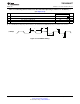
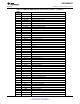
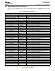
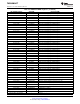
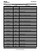
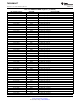
Table Of Contents
- 1 Digital Media System-on-Chip (DMSoC)
- Table of Contents
- 2 Revision History
- 3 Device Overview
- 3.1 Device Characteristics
- 3.2 Device Compatibility
- 3.3 ARM Subsystem
- 3.3.1 ARM926EJ-S RISC CPU
- 3.3.2 CP15
- 3.3.3 MMU
- 3.3.4 Caches and Write Buffer
- 3.3.5 Tightly Coupled Memory (TCM)
- 3.3.6 Advanced High-Performance Bus (AHB)
- 3.3.7 Embedded Trace Macrocell (ETM) and Embedded Trace Buffer (ETB)
- 3.3.8 ARM Memory Mapping
- 3.3.9 Peripherals
- 3.3.10 PLL Controller (PLLC)
- 3.3.11 Power and Sleep Controller (PSC)
- 3.3.12 ARM Interrupt Controller (AINTC)
- 3.3.13 System Module
- 3.3.14 Power Management
- 3.4 DSP Subsystem
- 3.5 Memory Map Summary
- 3.6 Pin Assignments
- 3.7 Terminal Functions
- 3.8 Device Support
- 3.9 Documentation Support
- 3.10 Community Resources
- 4 Device Configurations
- 4.1 System Module Registers
- 4.2 Power Considerations
- 4.3 Clock Considerations
- 4.4 Boot Sequence
- 4.5 Configurations At Reset
- 4.6 Configurations After Reset
- 4.7 Multiplexed Pin Configurations
- 4.7.1 Pin Muxing Selection At Reset
- 4.7.2 Pin Muxing Selection After Reset
- 4.7.3 Pin Multiplexing Details
- 4.7.3.1 PCI, HPI, EMIFA, and ATA Pin Muxing
- 4.7.3.2 PWM Signal Muxing
- 4.7.3.3 TSIF0 Input Signal Muxing (Serial/Parallel)
- 4.7.3.4 TSIF0 Output Signal Muxing (Serial/Parallel)
- 4.7.3.5 TSIF1 Input Signal Muxing (Serial Only)
- 4.7.3.6 TSIF1 Output Signal Muxing (Serial Only)
- 4.7.3.7 CRGEN Signal Muxing
- 4.7.3.8 UART0 Pin Muxing
- 4.7.3.9 UART1 Pin Muxing
- 4.7.3.10 UART2 Pin Muxing
- 4.7.3.11 ARM/DSP Communications Interrupts
- 4.7.3.12 Emulation Control
- 4.8 Debugging Considerations
- 5 System Interconnect
- 6 Device Operating Conditions
- 7 Peripheral Information and Electrical Specifications
- 7.1 Parameter Information
- 7.2 Recommended Clock and Control Signal Transition Behavior
- 7.3 Power Supplies
- 7.4 External Clock Input From DEV_MXI/DEV_CLKIN and AUX_MXI/AUX_CLKIN Pins
- 7.5 Clock PLLs
- 7.6 Enhanced Direct Memory Access (EDMA3) Controller
- 7.7 Reset
- 7.8 Interrupts
- 7.9 External Memory Interface (EMIF)
- 7.10 DDR2 Memory Controller
- 7.10.1 DDR2 Memory Controller Electrical Data/Timing
- 7.10.2 DDR2 Interface
- 7.10.2.1 DDR2 Interface Schematic
- 7.10.2.2 Compatible JEDEC DDR2 Devices
- 7.10.2.3 PCB Stackup
- 7.10.2.4 Placement
- 7.10.2.5 DDR2 Keep Out Region
- 7.10.2.6 Bulk Bypass Capacitors
- 7.10.2.7 High-Speed Bypass Capacitors
- 7.10.2.8 Net Classes
- 7.10.2.9 DDR2 Signal Termination
- 7.10.2.10 VREF Routing
- 7.10.2.11 DDR2 CK and ADDR_CTRL Routing
- 7.11 Video Port Interface (VPIF)
- 7.12 Transport Stream Interface (TSIF)
- 7.13 Clock Recovery Generator (CRGEN)
- 7.14 Video Data Conversion Engine (VDCE)
- 7.15 Peripheral Component Interconnect (PCI)
- 7.16 Ethernet MAC (EMAC)
- 7.17 Management Data Input/Output (MDIO)
- 7.18 Host-Port Interface (HPI) Peripheral
- 7.19 USB 2.0 [see Note]
- 7.20 ATA Controller
- 7.21 VLYNQ
- 7.22 Multichannel Audio Serial Port (McASP0/1) Peripherals
- 7.23 Serial Peripheral Interface (SPI)
- 7.24 Universal Asynchronouse Receiver/Transmitter (UART)
- 7.25 Inter-Integrated Circuit (I2C)
- 7.26 Pulse Width Modulator (PWM)
- 7.27 Timers
- 7.28 General-Purpose Input/Output (GPIO)
- 7.29 IEEE 1149.1 JTAG
- 8 Mechanical Packaging and Orderable Information
TMS320DM6467T
www.ti.com
SPRS605C –JULY 2009–REVISED JUNE 2012
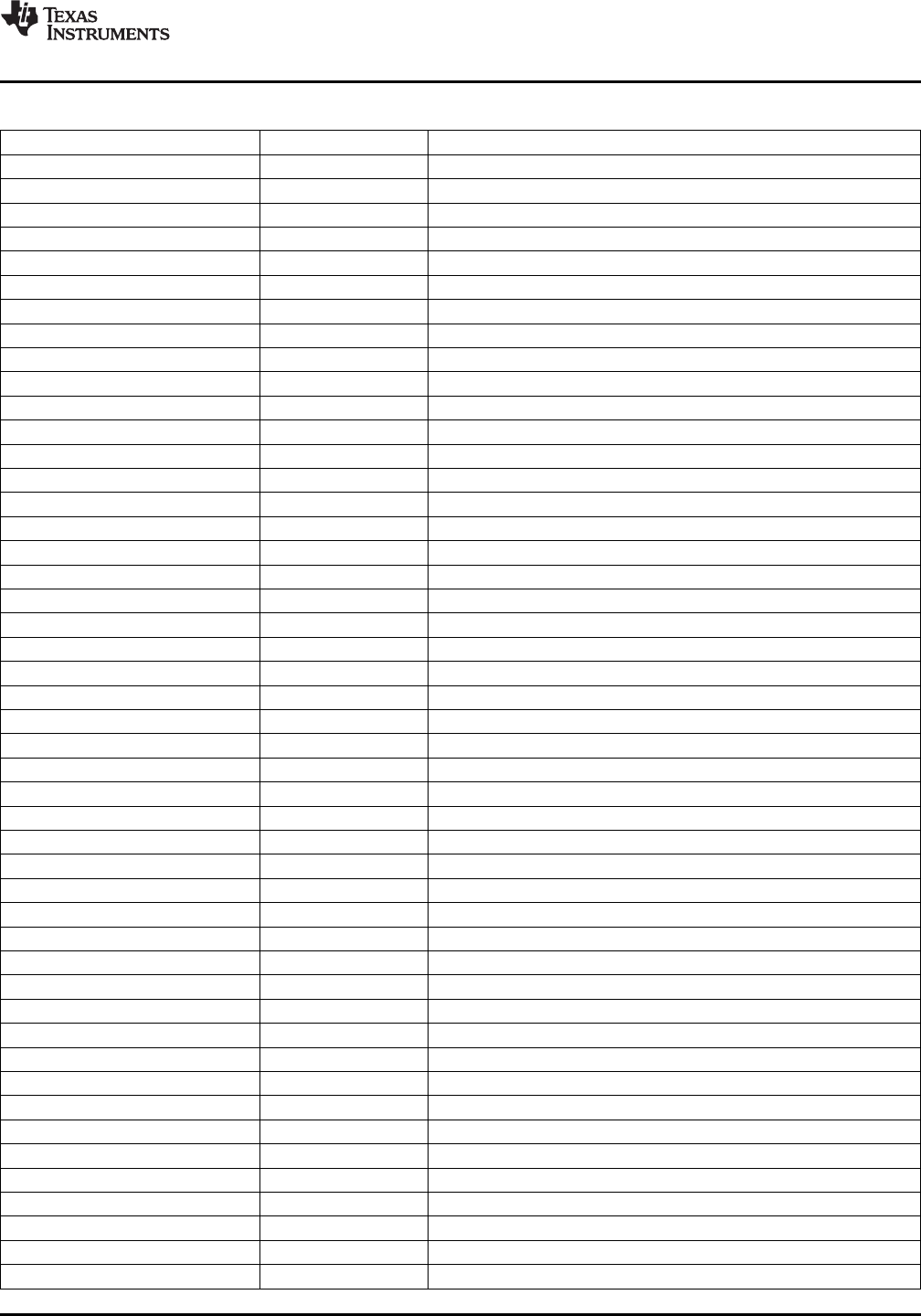
Table 7-16. DM6467T EDMA Registers (continued)
HEX ADDRESS RANGE ACRONYM REGISTER NAME
0x01C0 0300 EMR Event Missed Register
0x01C0 0304 EMRH Event Missed Register High
0x01C0 0308 EMCR Event Missed Clear Register
0x01C0 030C EMCRH Event Missed Clear Register High
0x01C0 0310 QEMR QDMA Event Missed Register
0x01C0 0314 QEMCR QDMA Event Missed Clear Register
0x01C0 0318 CCERR EDMA3CC Error Register
0x01C0 031C CCERRCLR EDMA3CC Error Clear Register
0x01C0 0320 EEVAL Error Evaluate Register
0x01C0 0324 - 0x01C0 033F – Reserved
0x01C0 0340 DRAE0 DMA Region Access Enable Register for Region 0
0x01C0 0344 DRAEH0 DMA Region Access Enable Register High for Region 0
0x01C0 0348 DRAE1 DMA Region Access Enable Register for Region 1
0x01C0 034C DRAEH1 DMA Region Access Enable Register High for Region 1
0x01C0 0350- 0x01C0 035F – Reserved
0x01C0 0360 DRAE4 DMA Region Access Enable Register for Region 4
0x01C0 0364 DRAEH4 DMA Region Access Enable Register High for Region 4
0x01C0 0368 DRAE5 DMA Region Access Enable Register for Region 5
0x01C0 036C DRAEH5 DMA Region Access Enable Register High for Region 5
0x01C0 0370 DRAE6 DMA Region Access Enable Register for Region 6
0x01C0 0374 DRAEH6 DMA Region Access Enable Register High for Region 6
0x01C0 0378 DRAE7 DMA Region Access Enable Register for Region 7
0x01C0 037C DRAEH7 DMA Region Access Enable Register High for Region 7
0x01C0 0380 QRAE0 QDMA Region Access Enable Register for Region 0
0x01C0 0384 QRAE1 QDMA Region Access Enable Register for Region 1
0x01C0 0388 - 0x01C0 038F – Reserved
0x01C0 0390 QRAE4 QDMA Region Access Enable Register for Region 4
0x01C0 0394 QRAE5 QDMA Region Access Enable Register for Region 5
0x01C0 0398 QRAE6 QDMA Region Access Enable Register for Region 6
0x01C0 039C QRAE7 QDMA Region Access Enable Register for Region 7
0x01C0 03A0 - 0x01C0 03FF – Reserved
0x01C0 0400 Q0E0 Event Q0 Entry 0 Register
0x01C0 0404 Q0E1 Event Q0 Entry 1 Register
0x01C0 0408 Q0E2 Event Q0 Entry 2 Register
0x01C0 040C Q0E3 Event Q0 Entry 3 Register
0x01C0 0410 Q0E4 Event Q0 Entry 4 Register
0x01C0 0414 Q0E5 Event Q0 Entry 5 Register
0x01C0 0418 Q0E6 Event Q0 Entry 6 Register
0x01C0 041C Q0E7 Event Q0 Entry 7 Register
0x01C0 0420 Q0E8 Event Q0 Entry 8 Register
0x01C0 0424 Q0E9 Event Q0 Entry 9 Register
0x01C0 0428 Q0E10 Event Q0 Entry 10 Register
0x01C0 042C Q0E11 Event Q0 Entry 11 Register
0x01C0 0430 Q0E12 Event Q0 Entry 12 Register
0x01C0 0434 Q0E13 Event Q0 Entry 13 Register
0x01C0 0438 Q0E14 Event Q0 Entry 14 Register
0x01C0 043C Q0E15 Event Q0 Entry 15 Register
Copyright © 2009–2012, Texas Instruments Incorporated Peripheral Information and Electrical Specifications 167
Submit Documentation Feedback
Product Folder Link(s): TMS320DM6467T