RM46L450 RM46L850 www.ti.com SPNS184A – SEPTEMBER 2012 – REVISED SEPTEMBER 2013 RM46Lx50 16- and 32-Bit RISC Flash Microcontroller Check for Samples: RM46L450, RM46L850 1 RM46Lx50 16- and 32-Bit RISC Flash Microcontroller 1.
RM46L450 RM46L850 SPNS184A – SEPTEMBER 2012 – REVISED SEPTEMBER 2013 1.2 • • 2 www.ti.
RM46L450 RM46L850 www.ti.com 1.3 SPNS184A – SEPTEMBER 2012 – REVISED SEPTEMBER 2013 Description The RM46Lx50 device is a high-performance microcontroller family for safety systems.
RM46L450 RM46L850 SPNS184A – SEPTEMBER 2012 – REVISED SEPTEMBER 2013 www.ti.com The device has multiple communication interfaces: three MibSPIs, two SPIs, one LIN, one SCI, three DCANs, one I2C, one Ethernet, and one USB module. The SPI provides a convenient method of serial high-speed communications between similar shift-register type devices. The LIN supports the Local Interconnect standard 2.0 and can be used as a UART in full-duplex mode using the standard NonReturn-to-Zero (NRZ) format.
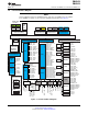
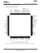
RM46L450 RM46L850 www.ti.com 1.4 SPNS184A – SEPTEMBER 2012 – REVISED SEPTEMBER 2013 Functional Block Diagram NOTE The block diagram reflects the 337BGA package. Some pins are multiplexed or not available in the 144QFP. For details, see the respective terminal functions tables in Section 2.3. 192kB RAM with ECC 32K 32K 32K 32K 32K 32K 1.
RM46L450 RM46L850 SPNS184A – SEPTEMBER 2012 – REVISED SEPTEMBER 2013 www.ti.com Table 1-1. Device Comparison Table 6 Orderable Part # Part # Flash RAM EMAC USB Package RM46L450PGET RM46L450 1MB 128kB 10/100 Host + Device 144-Pin QFP RM46L450ZWTT RM46L450 1MB 128kB 10/100 Host + Device 337-Ball Grid Array RM46L850PGET RM46L850 1.25MB 192kB 10/100 Host + Device 144-Pin QFP RM46L850ZWTT RM46L850 1.
RM46L450 RM46L850 www.ti.com 1 SPNS184A – SEPTEMBER 2012 – REVISED SEPTEMBER 2013 RM46Lx50 16- and 32-Bit RISC Flash Microcontroller .......................................... 1 ............................................. 1.2 Applications .......................................... 1.3 Description ........................................... 1.4 Functional Block Diagram ........................... Revision History .............................................. 2 Device Package and Terminal Functions ...
RM46L450 RM46L850 SPNS184A – SEPTEMBER 2012 – REVISED SEPTEMBER 2013 www.ti.com Revision History NOTE: Page numbers for previous revisions may differ from page numbers in the current version. This data manual revision history highlights the technical changes made to the initial revision of the device-specific data manual to make it an A revision. Document Revision History Section Change From To Section 3.1 Increased absolute max voltage VCCIO and Input Voltage 4.1 V 4.
RM46L450 RM46L850 www.ti.
RM46L450 RM46L850 SPNS184A – SEPTEMBER 2012 – REVISED SEPTEMBER 2013 2.2 www.ti.
RM46L450 RM46L850 www.ti.com 2.3 SPNS184A – SEPTEMBER 2012 – REVISED SEPTEMBER 2013 Terminal Functions Section 2.3.1 and Section 2.3.2 identify the external signal names, the associated pin/ball numbers along with the mechanical package designator, the pin/ball type (Input, Output, IO, Power or Ground), whether the pin/ball has any internal pullup/pulldown, whether the pin/ball can be configured as a GPIO, and a functional pin/ball description.
RM46L450 RM46L850 SPNS184A – SEPTEMBER 2012 – REVISED SEPTEMBER 2013 www.ti.com Table 2-1.
RM46L450 RM46L850 www.ti.com 2.3.1.2 SPNS184A – SEPTEMBER 2012 – REVISED SEPTEMBER 2013 Enhanced High-End Timer Modules (N2HET) Table 2-2. PGE Enhanced High-End Timer Modules (N2HET) Terminal Signal Name 144 PGE N2HET1[0]/SPI4CLK/EPWM2B 25 N2HET1[01]/SPI4NENA/USB2.TXEN/ USB_FUNC.PUENO/N2HET2[8]/EQEP2A 23 N2HET1[02]/SPI4SIMO[0]/EPWM3A 30 N2HET1[03]/SPI4NCS[0]/USB2.SPEED/ USB_FUNC.
RM46L450 RM46L850 SPNS184A – SEPTEMBER 2012 – REVISED SEPTEMBER 2013 www.ti.com Table 2-2. PGE Enhanced High-End Timer Modules (N2HET) (continued) Terminal Signal Name 144 PGE GIOA[2]/USB2.TXDAT/USB_FUNC.TXDO/N2HET2[0]/EQE P2I 9 GIOA[6]/N2HET2[4]/EPWM1B 16 GIOA[7]/N2HET2[6]EPWM2A 22 N2HET1[01]/SPI4NENA/USB2.TXEN/ USB_FUNC.PUENO//N2HET2[8] 23 N2HET1[03]/SPI4NCS[0]/USB2.SPEED/ USB_FUNC.PUENON/N2HET2[10]/EQEP2B 24 N2HET1[05]/SPI4SOMI[0]/N2HET2[12] 31 N2HET1[07]/USB2.PortPower/USB_FUNC.
RM46L450 RM46L850 www.ti.com 2.3.1.4 SPNS184A – SEPTEMBER 2012 – REVISED SEPTEMBER 2013 Enhanced Quadrature Encoder Pulse Modules (eQEP) Table 2-4.
RM46L450 RM46L850 SPNS184A – SEPTEMBER 2012 – REVISED SEPTEMBER 2013 2.3.1.5 www.ti.com Enhanced Pulse-Width Modulator Modules (ePWM) Table 2-5. PGE Enhanced Pulse-Width Modulator Modules (ePWM) Terminal Signal Name 144 PGE Signal Type Default Pull State Pull Type Output Pull Down - Description GIOA[5]/EXTCLKIN/EPWM1A/N2HET1_PIN_nDIS 14 GIOA[6]/N2HET2[4]/EPWM1B 16 Enhanced PWM1 Output B N2HET1[11]/MIBSPI3NCS[4]/N2HET2[18]/ USB2.OverCurrent/USB_FUNC.
RM46L450 RM46L850 www.ti.com 2.3.1.6 SPNS184A – SEPTEMBER 2012 – REVISED SEPTEMBER 2013 General-Purpose Input / Output (GPIO) Table 2-6. PGE General-Purpose Input / Output (GPIO) Terminal Signal Name 144 PGE GIOA[0]/USB2.VP/USB_FUNC.RXDPI 2 GIOA[1]/USB2.VM/USB_FUNC.RXDMI 5 GIOA[2]/USB2.TXDAT/USB_FUNC.TXDO/N2HET2[0]/EQEP 2II 9 GIOA[5]/EXTCLKIN/EPWM1A/N2HET1_PIN_nDIS 14 GIOA[6]/N2HET2[4]/EPWM1B 16 GIOA[7]/N2HET2[6]/EPWM2A 22 GIOB[0]/USB1.TXDAT 126 GIOB[1]/USB1.
RM46L450 RM46L850 SPNS184A – SEPTEMBER 2012 – REVISED SEPTEMBER 2013 2.3.1.9 www.ti.com Standard Serial Communication Interface (SCI) Table 2-9. PGE Standard Serial Communication Interface (SCI) Terminal Signal Name 144 PGE N2HET1[06]/SCIRX/EPWM5A 38 N2HET1[13]/SCITX/EPWM5B 39 Signal Type Default Pull State Pull Type I/O Pull Down Programmable, 20 µA Description SCI receive, or GPIO SCI transmit, or GPIO 2.3.1.10 Inter-Integrated Circuit Interface Module (I2C) Table 2-10.
RM46L450 RM46L850 www.ti.com SPNS184A – SEPTEMBER 2012 – REVISED SEPTEMBER 2013 2.3.1.12 Multi-Buffered Serial Peripheral Interface Modules (MibSPI) Table 2-12.
RM46L450 RM46L850 SPNS184A – SEPTEMBER 2012 – REVISED SEPTEMBER 2013 www.ti.com 2.3.1.13 Ethernet Controller Table 2-13. PGE Ethernet Controller: MDIO Interface Terminal Signal Name 144 PGE Signal Type Default Pull State Pull Type MIBSPI3NCS[1]/N2HET1[25]/MDCLK 37 Output Pull Up - MIBSPI1NCS[2]/N2HET1[19]/MDIO 40 I/O Pull Up Fixed, 20 µA Description Serial clock output Serial data input/output Table 2-14.
RM46L450 RM46L850 www.ti.com SPNS184A – SEPTEMBER 2012 – REVISED SEPTEMBER 2013 Table 2-15. PGE Ethernet Controller: Media Independent Interface (MII) (continued) Terminal Signal Name 144 PGE Signal Type Default Pull State Pull Type Output Pull Up - MIBSPI5SOMI[0]/MII_TXD[0]/RMII_TXD[0] 98 MIBSPI5SIMO[0]/MII_TXD[1] 99 MIBSPI1NCS[0]/MIBSPI1SOMI[1]/MII_TXD[2]/ USB1.RCV/ECAP6 105 N2HET1[08]/MIBSPI1SIMO[1]/MII_TXD[3]/ USB1.
RM46L450 RM46L850 SPNS184A – SEPTEMBER 2012 – REVISED SEPTEMBER 2013 www.ti.com Table 2-17. PGE USB Device Port Controller Interface (USB_FUNC) Terminal Signal Type Default Pull State Pull Type Description Output Pull Down - Pull Up enable, allows for software-programmable USB device connect/disconnect Signal Name 144 PGE N2HET1[07]/USB2.PortPower/USB_FUNC.GZO/N2HET2[14] 33 N2HET1[01]/SPI4NENA/USB2.TXEN/USB_FUNC.PUENO/ N2HET2[8] 23 N2HET1[03]/SPI4NCS[0]/USB2.SPEED/USB_FUNC.
RM46L450 RM46L850 www.ti.com SPNS184A – SEPTEMBER 2012 – REVISED SEPTEMBER 2013 Table 2-18. PGE System Module Interface (continued) Terminal Signal Name 144 PGE nERROR 117 Signal Type Default Pull State Pull Type I/O Pull Down 20 µA Description ESM Error Signal Indicates error of high severity. See Section 4.18. 2.3.1.16 Clock Inputs and Outputs Table 2-19.
RM46L450 RM46L850 SPNS184A – SEPTEMBER 2012 – REVISED SEPTEMBER 2013 www.ti.com 2.3.1.19 Supply for Core Logic: 1.2V nominal Table 2-22. PGE Supply for Core Logic: 1.2V nominal Terminal Signal Name 144 PGE VCC 17 VCC 29 VCC 45 VCC 48 VCC 49 VCC 57 VCC 87 VCC 101 VCC 114 VCC 123 VCC 137 VCC 143 Signal Type Default Pull State Pull Type 1.2V Power - None Description Core supply 2.3.1.20 Supply for I/O Cells: 3.3V nominal Table 2-23. PGE Supply for I/O Cells: 3.
RM46L450 RM46L850 www.ti.com SPNS184A – SEPTEMBER 2012 – REVISED SEPTEMBER 2013 2.3.1.21 Ground Reference for All Supplies Except VCCAD Table 2-24.
RM46L450 RM46L850 SPNS184A – SEPTEMBER 2012 – REVISED SEPTEMBER 2013 2.3.2 www.ti.com ZWT Package 2.3.2.1 Multi-Buffered Analog-to-Digital Converters (MibADC) Table 2-25.
RM46L450 RM46L850 www.ti.com 2.3.2.2 SPNS184A – SEPTEMBER 2012 – REVISED SEPTEMBER 2013 Enhanced High-End Timer Modules (N2HET) Table 2-26. ZWT Enhanced High-End Timer Modules (N2HET) Terminal Signal Name 337 ZWT N2HET1[0]/SPI4CLK/EPWM2B K18 N2HET1[01]/SPI4NENA/N2HET2[8] V2 N2HET1[02]/SPI4SIMO[0]/EPWM3A W5 N2HET1[03]/SPI4NCS[0]/USB2.SPEED/ USB_FUNC.
RM46L450 RM46L850 SPNS184A – SEPTEMBER 2012 – REVISED SEPTEMBER 2013 www.ti.com Table 2-26. ZWT Enhanced High-End Timer Modules (N2HET) (continued) Terminal Signal Name 337 ZWT GIOA[2]/USB2.TXDAT/USB_FUNC.TXDO/N2HET2[0]/EQEP 2I C1 EMIF_ADDR[0]/N2HET2[1] D4 GIOA[3]/N2HET2[2] E1 EMIF_ADDR[1]/N2HET2[3] D5 GIOA[6]/N2HET2[4]/EPWM1B H3 EMIF_BA[1]/N2HET2[5] D16 GIOA[7]/N2HET2[6]/EPWM2A M1 EMIF_nCS[0]/N2HET2[7] N17 N2HET1[01]/SPI4NENA/USB2.TXEN/ USB_FUNC.
RM46L450 RM46L850 www.ti.com 2.3.2.4 SPNS184A – SEPTEMBER 2012 – REVISED SEPTEMBER 2013 Enhanced Quadrature Encoder Pulse Modules (eQEP) Table 2-28.
RM46L450 RM46L850 SPNS184A – SEPTEMBER 2012 – REVISED SEPTEMBER 2013 2.3.2.5 www.ti.com Enhanced Pulse-Width Modulator Modules (ePWM) Table 2-29. ZWT Enhanced Pulse-Width Modulator Modules (ePWM) Terminal Signal Name 337 ZWT Signal Type Default Pull State Pull Type Output Pull Down - Description GIOA[5]/EXTCLKIN/EPWM1A/N2HET1_PIN_nDIS B5 GIOA[6]/N2HET2[4]/EPWM1B H3 Enhanced PWM1 Output B N2HET1[11]/MIBSPI3NCS[4]/N2HET2[18]/USB2.OverCurrent /USB_FUNC.
RM46L450 RM46L850 www.ti.com 2.3.2.6 SPNS184A – SEPTEMBER 2012 – REVISED SEPTEMBER 2013 General-Purpose Input / Output (GPIO) Table 2-30. ZWT General-Purpose Input / Output (GPIO) Terminal Signal Name 337 ZWT GIOA[0]/USB2.VP/USB_FUNC.RXDPI A5 GIOA[1]/USB2.VM/USB_FUNC.RXDMI C2 GIOA[2]/USB2.TXDAT/USB_FUNC.TXDO/N2HET2[0] /EQEP2I C1 GIOA[3]/N2HET2[2] E1 GIOA[4] A6 GIOA[5]/EXTCLKIN/EPWM1A/N2HET1_PIN_nDIS B5 GIOA[6]/N2HET2[4]/EPWM1B H3 GIOA[7]/N2HET2[6]/EPWM2A M1 GIOB[0]/USB1.
RM46L450 RM46L850 SPNS184A – SEPTEMBER 2012 – REVISED SEPTEMBER 2013 2.3.2.7 www.ti.com Controller Area Network Controllers (DCAN) Table 2-31. ZWT Controller Area Network Controllers (DCAN) Terminal Signal Name 337 ZWT Signal Type Default Pull State Pull Type I/O Pull Up Programmable, 20 µA Description CAN1RX B10 CAN1TX A10 CAN2RX H1 CAN2 receive, or GPIO CAN2TX H2 CAN2 transmit, or GPIO CAN3RX M19 CAN3 receive, or GPIO CAN3TX M18 CAN3 transmit, or GPIO 2.3.2.
RM46L450 RM46L850 www.ti.com SPNS184A – SEPTEMBER 2012 – REVISED SEPTEMBER 2013 2.3.2.10 Inter-Integrated Circuit Interface Module (I2C) Table 2-34. ZWT Inter-Integrated Circuit Interface Module (I2C) Terminal Signal Name 337 ZWT MIBSPI3NCS[2]/I2C_SDA/N2HET1[27]/nTZ2 B2 MIBSPI3NCS[3]/I2C_SCL/N2HET1[29]/nTZ1 C3 Signal Type Default Pull State Pull Type I/O Pull Up Programmable, 20 µA Description I2C serial data, or GPIO I2C serial clock, or GPIO 2.3.2.
RM46L450 RM46L850 SPNS184A – SEPTEMBER 2012 – REVISED SEPTEMBER 2013 www.ti.com 2.3.2.12 Multi-Buffered Serial Peripheral Interface Modules (MibSPI) Table 2-36. ZWT Multi-Buffered Serial Peripheral Interface Modules (MibSPI) Terminal Signal Name 337 ZWT MIBSPI1CLK F18 MIBSPI1NCS[0]/MIBSPI1SOMI[1]/MII_TXD[2]/ USB1.RCV R2 MIBSPI1NCS[1]/N2HET1[17]/MII_COL/ USB1.
RM46L450 RM46L850 www.ti.com SPNS184A – SEPTEMBER 2012 – REVISED SEPTEMBER 2013 Table 2-36. ZWT Multi-Buffered Serial Peripheral Interface Modules (MibSPI) (continued) Terminal Signal Name 337 ZWT MIBSPI5CLK/MII_TXEN/RMII_TXEN H19 MIBSPI5NCS[0]/EPWM4A E19 Signal Type Default Pull State Pull Type I/O Pull Up Programmable, 20 µA Description MibSPI5 clock, or GPIO MibSPI5 chip select, or GPIO MIBSPI5NCS[1] B6 MIBSPI5NCS[2] W6 MIBSPI5NCS[3] T12 MIBSPI5NENAMII_RXD[3]/ USB1.
RM46L450 RM46L850 SPNS184A – SEPTEMBER 2012 – REVISED SEPTEMBER 2013 www.ti.com 2.3.2.13 Ethernet Controller Table 2-37. ZWT Ethernet Controller: MDIO Interface Terminal Signal Name 337 ZWT Signal Type Default Pull State Pull Type MIBSPI3NCS[1]/N2HET1[25]/MDCLK V5 Output Pull Up - MIBSPI1NCS[2]/N2HET1[19]/MDIO G3 I/O Pull Up Fixed, 20 µA Description Serial clock output Serial data input/output Table 2-38.
RM46L450 RM46L850 www.ti.com SPNS184A – SEPTEMBER 2012 – REVISED SEPTEMBER 2013 Table 2-39. ZWT Ethernet Controller: Media Independent Interface (MII) (continued) Terminal Signal Name 337 ZWT Signal Type Default Pull State Pull Type Output Pull Up - MIBSPI5SOMI[0]/MII_TXD[0]/RMII_TXD[0] J18 MIBSPI5SIMO[0]/MII_TXD[1] J19 MIBSPI1NCS[0]/MIBSPI1SOMI[1]/MII_TXD[2]/ USB1.RCV R2 N2HET1[08]/MIBSPI1SIMO[1]/MII_TXD[3]/ USB1.
RM46L450 RM46L850 SPNS184A – SEPTEMBER 2012 – REVISED SEPTEMBER 2013 www.ti.com 2.3.2.14 USB Host Port Controller Interface Table 2-40. ZWT USB Host Port Controller Interface (USB1, USB2) Terminal Signal Name 337 ZWT Signal Type Default Pull State Pull Type Description Input Pull Down Fixed, 20 µA Overcurrent indication from USB power switch Pull Up Fixed, 20 µA Receive data from USB port transceiver N2HET1[08]/MIBSPI1SIMO[1]/MII_TXD[3]/ USB1.
RM46L450 RM46L850 www.ti.com SPNS184A – SEPTEMBER 2012 – REVISED SEPTEMBER 2013 Table 2-41. ZWT USB Device Port Controller Interface (USB_FUNC) (continued) Terminal Signal Name 337 ZWT Signal Type Default Pull State Pull Type Description Input Pull Down Fixed, 20 µA USB device single-ended data input GIOB[3]/USB2.RCV/USB_FUNC.RXDI W10 GIOA[1]/USB2.VM/USB_FUNC.RXDMI C2 USB device logic value of D-minus GIOA[0]/USB2.VP/USB_FUNC.RXDPI A5 USB device logic value of D-plus N2HET1[22]/USB2.
RM46L450 RM46L850 SPNS184A – SEPTEMBER 2012 – REVISED SEPTEMBER 2013 www.ti.com 2.3.2.15 External Memory Interface (EMIF) Table 2-42. External Memory Interface (EMIF) Terminal Signal Name 337 ZWT Signal Type Default Pull State Pull Type - - Description EMIF_CKE L3 Output EMIF_CLK K3 I/O EMIF_nWE/EMIF_RNW D17 Output EMIF_nOE E12 EMIF_nWAIT P3 I/O Pull Up Fixed, 20 µA EMIF Extended Wait Signal EMIF_nWE/EMIF_RNW D17 Output - - EMIF Write Enable.
RM46L450 RM46L850 www.ti.com SPNS184A – SEPTEMBER 2012 – REVISED SEPTEMBER 2013 Table 2-42.
RM46L450 RM46L850 SPNS184A – SEPTEMBER 2012 – REVISED SEPTEMBER 2013 www.ti.com 2.3.2.16 System Module Interface Table 2-43. ZWT System Module Interface Terminal Signal Name 337 ZWT Signal Type Default Pull State Pull Type Description nPORRST W7 Input Pull Down 100 µA Power-on reset, cold reset External power supply monitor circuitry must drive nPORRST low when any of the supplies to the microcontroller fall out of thespecified range. This terminal has a glitch filter. See Section 4.8.
RM46L450 RM46L850 www.ti.com SPNS184A – SEPTEMBER 2012 – REVISED SEPTEMBER 2013 2.3.2.18 Test and Debug Modules Interface Table 2-45.
RM46L450 RM46L850 SPNS184A – SEPTEMBER 2012 – REVISED SEPTEMBER 2013 www.ti.com Table 2-47. No Connects (continued) Terminal Signal Name 337 ZWT Signal Type Default Pull State Pull Type Description No Connects. These balls are not connected to any internal logic and can be connected to the PCB ground without affecting the functionality of the device.
RM46L450 RM46L850 www.ti.com SPNS184A – SEPTEMBER 2012 – REVISED SEPTEMBER 2013 Table 2-47. No Connects (continued) Terminal Signal Name 337 ZWT Signal Type Default Pull State Pull Type Description No Connects. These balls are not connected to any internal logic and can be connected to the PCB ground without affecting the functionality of the device.
RM46L450 RM46L850 SPNS184A – SEPTEMBER 2012 – REVISED SEPTEMBER 2013 www.ti.com 2.3.2.21 Supply for Core Logic: 1.2V nominal Table 2-48. ZWT Supply for Core Logic: 1.2V nominal Terminal Signal Name 337 ZWT VCC F9 VCC F10 VCC H10 VCC J14 VCC K6 VCC K8 VCC K12 VCC K14 VCC L6 VCC M10 VCC P10 46 Device Package and Terminal Functions Signal Type Default Pull State Pull Type 1.
RM46L450 RM46L850 www.ti.com SPNS184A – SEPTEMBER 2012 – REVISED SEPTEMBER 2013 2.3.2.22 Supply for I/O Cells: 3.3V nominal Table 2-49. ZWT Supply for I/O Cells: 3.
RM46L450 RM46L850 SPNS184A – SEPTEMBER 2012 – REVISED SEPTEMBER 2013 www.ti.com 2.3.2.23 Ground Reference for All Supplies Except VCCAD Table 2-50.
RM46L450 RM46L850 www.ti.com SPNS184A – SEPTEMBER 2012 – REVISED SEPTEMBER 2013 3 Device Operating Conditions 3.1 Absolute Maximum Ratings Over Operating Free-Air Temperature Range, (1) VCC (2) Supply voltage range: VCCIO, VCCP Input voltage range: Input clamp current: -0.3 V to 1.43 V (2) -0.3 V to 4.6 V VCCAD -0.3 V to 5.5 V All input pins, with exception of ADC pins -0.3 V to 4.6 V ADC input pins -0.3 V to 5.
RM46L450 RM46L850 SPNS184A – SEPTEMBER 2012 – REVISED SEPTEMBER 2013 3.3 www.ti.com Switching Characteristics over Recommended Operating Conditions for Clock Domains Table 3-1.
RM46L450 RM46L850 www.ti.com 3.
RM46L450 RM46L850 SPNS184A – SEPTEMBER 2012 – REVISED SEPTEMBER 2013 3.6 www.ti.com Input/Output Electrical Characteristics Over Recommended Operating Conditions (1) PARAMETER TEST CONDITIONS MIN TYP MAX UNIT Vhys Input hysteresis All inputs 180 mV VIL Low-level input voltage All inputs -0.3 0.8 V VIH High-level input voltage All inputs 2 VCCIO + 0.
RM46L450 RM46L850 www.ti.com 3.7 SPNS184A – SEPTEMBER 2012 – REVISED SEPTEMBER 2013 Output Buffer Drive Strengths Table 3-2.
RM46L450 RM46L850 SPNS184A – SEPTEMBER 2012 – REVISED SEPTEMBER 2013 www.ti.com Table 3-3. Selectable 8 mA/2 mA Control (continued) Signal Control Bit Address 8 mA 2 mA SPI2SIMO SPI2PC9[10] (1) 0xFFF7 F668 0 1 SPI2SOMI (1) 0xFFF7 F668 0 1 3.8 SPI2PC9[11] Input Timings t pw Input V IH VCCIO VIH VIL V IL 0 Figure 3-2. TTL-Level Inputs Table 3-4.
RM46L450 RM46L850 www.ti.com SPNS184A – SEPTEMBER 2012 – REVISED SEPTEMBER 2013 Table 3-5. Switching Characteristics for Output Timings versus Load Capacitance (CL) (continued) Parameter Rise time, tr Selectable 8 mA / 2 mA-z pins (see Table 3-2) MIN 8 mA mode Fall time, tf Rise time, tr 2 mA-z mode Fall time, tf CL = 15 pF ns 4 CL = 100 pF 7.2 CL = 150 pF 12.5 CL = 15 pF 2.5 CL = 50 pF 4 CL = 100 pF 7.2 CL = 150 pF 12.
RM46L450 RM46L850 SPNS184A – SEPTEMBER 2012 – REVISED SEPTEMBER 2013 www.ti.com 3.10 Low-EMI Output Buffers The low-EMI output buffer has been designed explicitly to address the issue of decoupling sources of emissions from the pins which they drive. This is accomplished by adaptively controlling the impedance of the output buffer, and is particularly effective with capacitive loads.
RM46L450 RM46L850 www.ti.com SPNS184A – SEPTEMBER 2012 – REVISED SEPTEMBER 2013 4 System Information and Electrical Specifications 4.1 Device Power Domains The device core logic is split up into multiple power domains in order to optimize the power for a given application use case. There are 6 power domains in total: PD1, PD2, PD3, PD5, RAM_PD1, and RAM_PD2. Refer to Section 1.4 for more information. PD1 is an "always-ON" power domain, which cannot be turned off.
RM46L450 RM46L850 SPNS184A – SEPTEMBER 2012 – REVISED SEPTEMBER 2013 www.ti.com Table 4-1. Voltage Monitoring Specifications PARAMETER VMON 4.2.3 Voltage monitoring thresholds MIN TYP MAX UNIT VCC low - VCC level below this threshold is detected as too low. 0.75 0.9 1.13 V VCC high - VCC level above this threshold is detected as too high. 1.40 1.7 2.1 VCCIO low - VCCIO level below this threshold is detected as too low. 1.85 2.4 2.
RM46L450 RM46L850 www.ti.com 4.3 SPNS184A – SEPTEMBER 2012 – REVISED SEPTEMBER 2013 Power Sequencing and Power On Reset 4.3.1 Power-Up Sequence There is no timing dependency between the ramp of the VCCIO and the VCC supply voltage. The powerup sequence starts with the I/O voltage rising above the minimum I/O supply threshold, (see Table 4-4 for more details), core voltage rising above the minimum core supply threshold and the release of power-on reset.
RM46L450 RM46L850 SPNS184A – SEPTEMBER 2012 – REVISED SEPTEMBER 2013 www.ti.com Table 4-4. Electrical Requirements for nPORRST (continued) NO Parameter tf(nPORRST) Filter time nPORRST pin; MIN MAX Unit 475 2000 ns pulses less than MIN will be filtered out, pulses greater than MAX will generate a reset. 3.3 V 1.2 V VCCIOPORH VCCPORH 6 VCCIOPORL VCC (1.2 V) VCCIO / VCCP(3.
RM46L450 RM46L850 www.ti.com 4.4 SPNS184A – SEPTEMBER 2012 – REVISED SEPTEMBER 2013 Warm Reset (nRST) This is a bidirectional reset signal. The internal circuitry drives the signal low on detecting any device reset condition. An external circuit can assert a device reset by forcing the signal low. On this terminal, the output buffer is implemented as an open drain (drives low only).
RM46L450 RM46L850 SPNS184A – SEPTEMBER 2012 – REVISED SEPTEMBER 2013 4.5 4.5.1 www.ti.com ARM© Cortex-R4F™ CPU Information Summary of ARM Cortex-R4F™ CPU Features The features of the ARM Cortex-R4F™ CPU include: • An integer unit with integral EmbeddedICE-RT logic. • High-speed Advanced Microprocessor Bus Architecture (AMBA) Advanced eXtensible Interfaces (AXI) for Level two (L2) master and slave interfaces.
RM46L450 RM46L850 www.ti.com 4.5.4 SPNS184A – SEPTEMBER 2012 – REVISED SEPTEMBER 2013 Duplicate clock tree after GCLK The CPU clock domain is split into two clock trees, one for each CPU, with the clock of the 2nd CPU running at the same frequency and in phase to the clock of CPU1. See Figure 4-3. 4.5.5 ARM Cortex-R4F™ CPU Compare Module (CCM-R4) for Safety This device has two ARM Cortex-R4F™ CPU cores, where the output signals of both CPUs are compared in the CCM-R4 unit.
RM46L450 RM46L850 SPNS184A – SEPTEMBER 2012 – REVISED SEPTEMBER 2013 4.5.6.1 1. 2. 3. 4. 5. 6. 7. www.ti.com Application Sequence for CPU Self-Test Configure clock domain frequencies. Select number of test intervals to be run. Configure the timeout period for the self-test run. Enable self-test. Wait for CPU reset. In the reset handler, read CPU self-test status to identify any failures. Retrieve CPU state if required. For more information see the device Technical Reference Manual. 4.5.6.
RM46L450 RM46L850 www.ti.com 4.6 SPNS184A – SEPTEMBER 2012 – REVISED SEPTEMBER 2013 Clocks 4.6.1 Clock Sources The table below lists the available clock sources on the device. Each of the clock sources can be enabled or disabled using the CSDISx registers in the system module. The clock source number in the table corresponds to the control bit in the CSDISx register for that clock source. The table also shows the default state of each clock source. Table 4-8.
RM46L450 RM46L850 SPNS184A – SEPTEMBER 2012 – REVISED SEPTEMBER 2013 www.ti.com 4.6.1.1.1 Timing Requirements for Main Oscillator Table 4-9.
RM46L450 RM46L850 www.ti.com 4.6.1.2 SPNS184A – SEPTEMBER 2012 – REVISED SEPTEMBER 2013 Low Power Oscillator The Low Power Oscillator (LPO) is comprised of two oscillators — HF LPO and LF LPO, in a single macro. 4.6.1.2.1 Features The main features of the LPO are: • Supplies a clock at extremely low power for power-saving modes. This is connected as clock source # 4 of the Global Clock Module. • Supplies a high-frequency clock for non-timing-critical systems.
RM46L450 RM46L850 SPNS184A – SEPTEMBER 2012 – REVISED SEPTEMBER 2013 4.6.1.3 www.ti.com Phase Locked Loop (PLL) Clock Modules The PLL is used to multiply the input frequency to some higher frequency. The main features of the PLL are: • Frequency modulation can be optionally superimposed on the synthesized frequency of PLL1. The frequency modulation capability of PLL2 is permanently disabled. • Configurable frequency multipliers and dividers. • Built-in PLL Slip monitoring circuit.
RM46L450 RM46L850 www.ti.com 4.6.1.4 SPNS184A – SEPTEMBER 2012 – REVISED SEPTEMBER 2013 External Clock Inputs The device supports up to two external clock inputs. This clock input must be a square wave input. The electrical and timing requirements for these clock inputs are specified below. The external clock sources are not checked for validity. They are assumed valid when enabled. Table 4-12.
RM46L450 RM46L850 SPNS184A – SEPTEMBER 2012 – REVISED SEPTEMBER 2013 www.ti.com Table 4-13. Clock Domain Descriptions (continued) Clock Domain Name Default Clock Source Clock Source Selection Register Description VCLKA2 VCLK VCLKASRC • • Defaults to VCLK as the source Is disabled via the CDDISx registers bit 5 VCLKA3_S VCLK VCLKACON • • • Defaults to VCLK as the source Frequency can be as fast as HCLK frequency.
RM46L450 RM46L850 www.ti.com 4.6.2.2 SPNS184A – SEPTEMBER 2012 – REVISED SEPTEMBER 2013 Mapping of Clock Domains to Device Modules Each clock domain has a dedicated functionality as shown in the figures below. GCM 0 OSCIN PLL #1 X1..256 /1..64 Low Power Oscillator GCLK, GCLK2 (to CPU) (FMzPLL) 1 * /1..32 /1..8 80kHz 4 10MHz 5 VCLK_sys (VCLK to system modules) PLL # 2 (FMzPLL) /1..64 X1..256 * the frequency at this node must not exceed the maximum HCLK specifiation.
RM46L450 RM46L850 SPNS184A – SEPTEMBER 2012 – REVISED SEPTEMBER 2013 4.6.2.3 www.ti.com Special Clock Source Selection Scheme for VCLKA4_DIVR_EMAC Some applications may need to use both the of Ethernet interfaces. The MII interface requires VCLKA4_DIVR_EMAC to be 25MHz and the RMII requires VCLKA4_DIVR_EAMC to be 50MHz. These different frequencies are supported by adding special dedicated clock source selection options for the VCLKA4_DIVR_EMAC clock domain. This logic is shown in .
RM46L450 RM46L850 www.ti.com 4.6.3 SPNS184A – SEPTEMBER 2012 – REVISED SEPTEMBER 2013 Clock Test Mode The RM4x platform architecture defines a special mode that allows various clock signals to be brought out on to the ECLK pin and N2HET1[12] device outputs. This mode is called the Clock Test mode. It is very useful for debugging purposes and can be configured via the CLKTEST register in the system module. Table 4-15.
RM46L450 RM46L850 SPNS184A – SEPTEMBER 2012 – REVISED SEPTEMBER 2013 4.7 www.ti.com Clock Monitoring The LPO Clock Detect (LPOCLKDET) module consists of a clock monitor (CLKDET) and an internal low power oscillator (LPO). The LPO provides two different clock sources – a low frequency (LFLPO) and a high frequency (HFLPO). The CLKDET is a supervisor circuit for an externally supplied clock signal (OSCIN).
RM46L450 RM46L850 www.ti.com 4.7.3.2 SPNS184A – SEPTEMBER 2012 – REVISED SEPTEMBER 2013 Mapping of DCC Clock Source Inputs Table 4-16. DCC1 Counter 0 Clock Sources CLOCK SOURCE [3:0] CLOCK NAME others oscillator (OSCIN) 0x5 high frequency LPO 0xA test clock (TCK) Table 4-17.
RM46L450 RM46L850 SPNS184A – SEPTEMBER 2012 – REVISED SEPTEMBER 2013 4.8 www.ti.com Glitch Filters A glitch filter is present on the following signals. Table 4-20.
RM46L450 RM46L850 www.ti.com 4.9 4.9.1 SPNS184A – SEPTEMBER 2012 – REVISED SEPTEMBER 2013 Device Memory Map Memory Map Diagram The figure below shows the device memory map.
RM46L450 RM46L850 SPNS184A – SEPTEMBER 2012 – REVISED SEPTEMBER 2013 4.9.2 www.ti.com Memory Map Table Please refer to and for a block diagrams showing the devices interconnect. Table 4-21. Device Memory Map FRAME ADDRESS RANGE MODULE NAME FRAME CHIP SELECT TCM Flash CS0 0x0000_0000 0x00FF_FFFF 16MB 1.25MB TCM RAM + RAM ECC CSRAM0 0x0800_0000 0x0BFF_FFFF 64MB 192kB Mirrored Flash Flash mirror frame 0x2000_0000 0x20FF_FFFF 16MB 1.
RM46L450 RM46L850 www.ti.com SPNS184A – SEPTEMBER 2012 – REVISED SEPTEMBER 2013 Table 4-21.
RM46L450 RM46L850 SPNS184A – SEPTEMBER 2012 – REVISED SEPTEMBER 2013 www.ti.com Table 4-21. Device Memory Map (continued) MODULE NAME FRAME CHIP SELECT FRAME ADDRESS RANGE START END FRAME ACTUAL SIZE SIZE MIBADC1 RAM PCS[31] 0xFF3E_0000 0xFF3F_FFFF 8kB Wrap around for accesses to unimplemented address offsets lower than 0x1FFF. Abort generated for accesses beyond 0x1FFF. 384B Look-Up Table for ADC1 wrapper. Starts at address offset 0x2000 and ends at address offset 0x217F.
RM46L450 RM46L850 www.ti.com SPNS184A – SEPTEMBER 2012 – REVISED SEPTEMBER 2013 Table 4-21.
RM46L450 RM46L850 SPNS184A – SEPTEMBER 2012 – REVISED SEPTEMBER 2013 4.9.3 www.ti.com Special Consideration for CPU Access Errors Resulting in Imprecise Aborts Any CPU write access to a Normal or Device type memory, which generates a fault, will generate an imprecise abort. The imprecise abort exception is disabled by default and must be enabled for the CPU to handle this exception. The imprecise abort handling is enabled by clearing the "A" bit in the CPU’s program status register (CPSR). 4.9.
RM46L450 RM46L850 www.ti.com • SPNS184A – SEPTEMBER 2012 – REVISED SEPTEMBER 2013 When POM is used to overlay the flash on to internal or external RAM, there is a bus contention possibility when another master accesses the TCM flash. This results in a system hang. – The POM implements a timeout feature to detect this exact scenario. The timeout needs to be enabled whenever POM overlay is enabled.
RM46L450 RM46L850 SPNS184A – SEPTEMBER 2012 – REVISED SEPTEMBER 2013 www.ti.com 4.10 Flash Memory 4.10.1 Flash Memory Configuration Flash Bank: A separate block of logic consisting of 1 to 16 sectors. Each flash bank normally has a customer-OTP and a TI-OTP area. These flash sectors share input/output buffers, data paths, sense amplifiers, and control logic. Flash Sector: A contiguous region of flash memory which must be erased simultaneously due to physical construction constraints.
RM46L450 RM46L850 www.ti.com SPNS184A – SEPTEMBER 2012 – REVISED SEPTEMBER 2013 4.10.3 ECC Protection for Flash Accesses All accesses to the program flash memory are protected by Single Error Correction Double Error Detection (SECDED) logic embedded inside the CPU. The flash module provides 8 bits of ECC code for 64 bits of instructions or data fetched from the flash memory.
RM46L450 RM46L850 SPNS184A – SEPTEMBER 2012 – REVISED SEPTEMBER 2013 www.ti.com 4.10.5 Program Flash Table 4-24. Timing Requirements for Program Flash Parameter tprog(144bit) Wide Word (144bit) programming time tprog(Total) 1.25MByte programming time (1) terase(bank0) Sector/Bank erase time (2) MIN (1) (2) MAX Unit 40 300 µs 13 s 6.6 s -40°C to 105°C 0°C to 60°C, for first 25 cycles 3.3 -40°C to 105°C 0.
RM46L450 RM46L850 www.ti.com SPNS184A – SEPTEMBER 2012 – REVISED SEPTEMBER 2013 4.11 Tightly-Coupled RAM Interface Module Figure 4-11 illustrates the connection of the Tightly Coupled RAM (TCRAM) to the Cortex-R4F™ CPU.
RM46L450 RM46L850 SPNS184A – SEPTEMBER 2012 – REVISED SEPTEMBER 2013 www.ti.com The parity protection for peripheral RAMs is not enabled by default and must be enabled by the application. Each individual peripheral contains control registers to enable the parity protection for accesses to its RAM. NOTE The CPU read access gets the actual data from the peripheral. The application can choose to generate an interrupt whenever a peripheral RAM parity error is detected.
RM46L450 RM46L850 www.ti.com SPNS184A – SEPTEMBER 2012 – REVISED SEPTEMBER 2013 4.13 On-Chip SRAM Initialization and Testing 4.13.1 On-Chip SRAM Self-Test Using PBIST 4.13.1.1 Features • • • Extensive instruction set to support various memory test algorithms ROM-based algorithms allow application to run TI production-level memory tests Independent testing of all on-chip SRAM 4.13.1.2 PBIST RAM Groups Table 4-26.
RM46L450 RM46L850 SPNS184A – SEPTEMBER 2012 – REVISED SEPTEMBER 2013 www.ti.com 4.13.2 On-Chip SRAM Auto Initialization This microcontroller allows some of the on-chip memories to be initialized via the Memory Hardware Initialization mechanism in the System module. This hardware mechanism allows an application to program the memory arrays with error detection capability to a known state based on their error detection scheme (odd/even parity or ECC).
RM46L450 RM46L850 www.ti.com SPNS184A – SEPTEMBER 2012 – REVISED SEPTEMBER 2013 4.14 External Memory Interface (EMIF) 4.14.1 Features The EMIF includes many features to enhance the ease and flexibility of connecting to external asynchronous memories or SDRAM devices.
RM46L450 RM46L850 SPNS184A – SEPTEMBER 2012 – REVISED SEPTEMBER 2013 EMIF_nCS[3:2] SETUP www.ti.com Extended Due to EMIF_WAIT STROBE STROBE HOLD EMIF_BA[1:0] EMIF_ADDR[21:0] EMIF_DATA[15:0] 14 11 EMIF_nOE 2 EMIF_WAIT 2 Asserted Deasserted Figure 4-13. EMIFnWAIT Read Timing Requirements 15 1 EMIF_nCS[3:2] EMIF_BA[1:0] EMIF_ADDR[21:0] EMIF_nDQM[1:0] 16 17 18 19 20 22 24 21 23 EMIF_nWE 27 26 EMIF_DATA[15:0] EMIF_nOE Figure 4-14.
RM46L450 RM46L850 www.ti.com SPNS184A – SEPTEMBER 2012 – REVISED SEPTEMBER 2013 SETUP Extended Due to EMIF_WAIT STROBE STROBE HOLD EMIF_nCS[3:2] EMIF_BA[1:0] EMIF_ADDR[21:0] EMIF_DATA[15:0] 28 25 EMIF_nWE 2 EMIF_WAIT 2 Asserted Deasserted Figure 4-15. EMIFnWAIT Write Timing Requirements Table 4-28. EMIF Asynchronous Memory Timing Requirements NO.
RM46L450 RM46L850 SPNS184A – SEPTEMBER 2012 – REVISED SEPTEMBER 2013 www.ti.com Table 4-29.
RM46L450 RM46L850 www.ti.com SPNS184A – SEPTEMBER 2012 – REVISED SEPTEMBER 2013 Table 4-29.
RM46L450 RM46L850 SPNS184A – SEPTEMBER 2012 – REVISED SEPTEMBER 2013 www.ti.com 4.14.2.2 Synchronous Timing BASIC SDRAM READ OPERATION 1 2 2 EMIF_CLK 4 3 EMIF_nCS[0] 6 5 EMIF_nDQM[1:0] 7 8 7 8 EMIF_BA[1:0] EMIF_ADDR[21:0] 19 2 EM_CLK Delay 17 20 18 EMIF_DATA[15:0] 11 12 EMIF_nRAS 13 14 EMIF_nCAS EMIF_nWE Figure 4-16.
RM46L450 RM46L850 www.ti.com SPNS184A – SEPTEMBER 2012 – REVISED SEPTEMBER 2013 BASIC SDRAM WRITE OPERATION 1 2 2 EMIF_CLK 4 3 EMIF_CS[0] 6 5 EMIF_DQM[1:0] 7 8 7 8 EMIF_BA[1:0] EMIF_ADDR[21:0] 9 10 EMIF_DATA[15:0] 11 12 EMIF_nRAS 13 EMIF_nCAS 15 16 EMIF_nWE Figure 4-17. Basic SDRAM Write Operation Table 4-30. EMIF Synchronous Memory Timing Requirements NO.
RM46L450 RM46L850 SPNS184A – SEPTEMBER 2012 – REVISED SEPTEMBER 2013 www.ti.com Table 4-31. EMIF Synchronous Memory Switching Characteristics (continued) 98 NO.
RM46L450 RM46L850 www.ti.com SPNS184A – SEPTEMBER 2012 – REVISED SEPTEMBER 2013 4.15 Vectored Interrupt Manager The vectored interrupt manager (VIM) provides hardware assistance for prioritizing and controlling the many interrupt sources present on this device. Interrupts are caused by events outside of the normal flow of program execution.
RM46L450 RM46L850 SPNS184A – SEPTEMBER 2012 – REVISED SEPTEMBER 2013 www.ti.com Table 4-32.
RM46L450 RM46L850 www.ti.com SPNS184A – SEPTEMBER 2012 – REVISED SEPTEMBER 2013 Table 4-32.
RM46L450 RM46L850 SPNS184A – SEPTEMBER 2012 – REVISED SEPTEMBER 2013 www.ti.com NOTE The EMIF_nWAIT signal has a pull-up on it. The EMIF module generates a "Wait Rise" interrupt whenever it detects a rising edge on the EMIF_nWAIT signal. This interrupt condition is indicated as soon as the device is powered up. This can be ignored if the EMIF_nWAIT signal is not used in the application.
RM46L450 RM46L850 www.ti.com SPNS184A – SEPTEMBER 2012 – REVISED SEPTEMBER 2013 4.16 DMA Controller The DMA controller is used to transfer data between two locations in the memory map in the background of CPU operations. Typically, the DMA is used to: • Transfer blocks of data between external and internal data memories • Restructure portions of internal data memory • Continually service a peripheral 4.16.
RM46L450 RM46L850 SPNS184A – SEPTEMBER 2012 – REVISED SEPTEMBER 2013 www.ti.com 4.16.2 Default DMA Request Map The DMA module on this microcontroller has 16 channels and up to 32 hardware DMA requests. The module contains DREQASIx registers which are used to map the DMA requests to the DMA channels. By default, channel 0 is mapped to request 0, channel 1 to request 1, and so on. Some DMA requests have multiple sources, as shown in Table 4-33.
RM46L450 RM46L850 www.ti.com SPNS184A – SEPTEMBER 2012 – REVISED SEPTEMBER 2013 Table 4-33.
RM46L450 RM46L850 SPNS184A – SEPTEMBER 2012 – REVISED SEPTEMBER 2013 www.ti.com 4.17 Real Time Interrupt Module The real-time interrupt (RTI) module provides timer functionality for operating systems and for benchmarking code. The RTI module can incorporate several counters that define the timebases needed for scheduling an operating system.
RM46L450 RM46L850 www.ti.com SPNS184A – SEPTEMBER 2012 – REVISED SEPTEMBER 2013 31 0 Update compare RTIUDCPy + 31 0 Compare DMAREQy RTICOMPy From counter block 0 = INTy From counter block 1 Compare control Figure 4-19. Compare Block Diagram 4.17.3 Clock Source Options The RTI module uses the RTI1CLK clock domain for generating the RTI time bases. The application can select the clock source for the RTI1CLK by configuring the RCLKSRC register in the System module at address 0xFFFFFF50.
RM46L450 RM46L850 SPNS184A – SEPTEMBER 2012 – REVISED SEPTEMBER 2013 www.ti.com 4.18 Error Signaling Module The Error Signaling Module (ESM) manages the various error conditions on the RM4x microcontroller. The error condition is handled based on a fixed severity level assigned to it. Any severe error condition can be configured to drive a low level on a dedicated device terminal called nERROR. This can be used as an indicator to an external monitor circuit to put the system into a safe state. 4.18.
RM46L450 RM46L850 www.ti.com SPNS184A – SEPTEMBER 2012 – REVISED SEPTEMBER 2013 Table 4-36.
RM46L450 RM46L850 SPNS184A – SEPTEMBER 2012 – REVISED SEPTEMBER 2013 www.ti.com Table 4-36.
RM46L450 RM46L850 www.ti.com SPNS184A – SEPTEMBER 2012 – REVISED SEPTEMBER 2013 Table 4-36.
RM46L450 RM46L850 SPNS184A – SEPTEMBER 2012 – REVISED SEPTEMBER 2013 www.ti.com 4.19 Reset / Abort / Error Sources Table 4-37. Reset/Abort/Error Sources ERROR SOURCE SYSTEM MODE ERROR RESPONSE ESM HOOKUP group.
RM46L450 RM46L850 www.ti.com SPNS184A – SEPTEMBER 2012 – REVISED SEPTEMBER 2013 Table 4-37. Reset/Abort/Error Sources (continued) ERROR SOURCE SYSTEM MODE ERROR RESPONSE ESM HOOKUP group.channel ESM 1.7 ESM 1.34 ESM 1.43 ESM 1.
RM46L450 RM46L850 SPNS184A – SEPTEMBER 2012 – REVISED SEPTEMBER 2013 www.ti.com Table 4-37. Reset/Abort/Error Sources (continued) ERROR SOURCE SYSTEM MODE ERROR RESPONSE ESM HOOKUP group.
RM46L450 RM46L850 www.ti.com SPNS184A – SEPTEMBER 2012 – REVISED SEPTEMBER 2013 4.20 Digital Windowed Watchdog This device includes a digital windowed watchdog (DWWD) module that protects against runaway code execution. The DWWD module allows the application to configure the time window within which the DWWD module expects the application to service the watchdog. A watchdog violation occurs if the application services the watchdog outside of this window, or fails to service the watchdog at all.
RM46L450 RM46L850 SPNS184A – SEPTEMBER 2012 – REVISED SEPTEMBER 2013 www.ti.com 4.21 Debug Subsystem 4.21.1 Block Diagram The device contains an ICEPICK module to allow JTAG access to the scan chains. Boundary Scan BSR/BSDL Boundary Scan I/F TRST TMS TCK RTCK TDI TDO Debug ROM1 Debug APB DAP Secondary Tap 0 APB Mux AHB-AP POM ICEPICK_C to SCR1 via A2A from PCR1/Bridge APB slave Cortex R4F Secondary Tap 2 AJSM Test Tap 0 eFuse Farm Test Tap 1 PSCON Figure 4-20.
RM46L450 RM46L850 www.ti.com SPNS184A – SEPTEMBER 2012 – REVISED SEPTEMBER 2013 Table 4-39.
RM46L450 RM46L850 SPNS184A – SEPTEMBER 2012 – REVISED SEPTEMBER 2013 www.ti.com 4.21.5 JTAG Scan Interface Timings Table 4-40. JTAG Scan Interface Timing (1) No.
RM46L450 RM46L850 www.ti.com SPNS184A – SEPTEMBER 2012 – REVISED SEPTEMBER 2013 4.21.6 Advanced JTAG Security Module This device includes a an Advanced JTAG Security Module (AJSM). which provides maximum security to the device’s memory content by allowing users to secure the device after programming. Flash Module Output OTP Contents (example) H L H ... ...
RM46L450 RM46L850 SPNS184A – SEPTEMBER 2012 – REVISED SEPTEMBER 2013 www.ti.com 4.21.7 Boundary Scan Chain The device supports BSDL-compliant boundary scan for testing pin-to-pin compatibility. The boundary scan chain is connected to the Boundary Scan Interface of the ICEPICK module. Device Pins (conceptual) RTCK TDI TDO IC E P ICK TRST TMS TCK Boundary Scan Interface Boundary Scan TDI TDO BSDL Figure 4-23.
RM46L450 RM46L850 www.ti.com SPNS184A – SEPTEMBER 2012 – REVISED SEPTEMBER 2013 5 Peripheral Information and Electrical Specifications 5.1 Enhanced Translator PWM Modules (ePWM) Figure 5-1 illustrates the connections between the seven ePWM modules (ePWM1,2,3,4,5,6,7) on the device.
RM46L450 RM46L850 SPNS184A – SEPTEMBER 2012 – REVISED SEPTEMBER 2013 5.1.1 www.ti.com ePWM Clocking and Reset Each ePWM module has a clock enable (EPWMxENCLK). When SYS_nRST is active low, the clock enables are ignored and the ePWM logic is clocked so that it can reset to a proper state. When SYS_nRST goes in-active high, the state of clock enable is respected. Table 5-1.
RM46L450 RM46L850 www.ti.com 5.1.4 SPNS184A – SEPTEMBER 2012 – REVISED SEPTEMBER 2013 Phase-Locking the Time-Base Clocks of Multiple ePWM Modules The TBCLKSYNC bit can be used to globally synchronize the time-base clocks of all enabled ePWM modules on a device. This bit is implemented as PINMMR37 register bit 1. When TBCLKSYNC = 0, the time-base clock of all ePWM modules is stopped. This is the default condition.
RM46L450 RM46L850 SPNS184A – SEPTEMBER 2012 – REVISED SEPTEMBER 2013 www.ti.com Table 5-3.
RM46L450 RM46L850 www.ti.com SPNS184A – SEPTEMBER 2012 – REVISED SEPTEMBER 2013 Table 5-5. ePWMx Switching Characteristics (continued) PARAMETER td(TZ- TEST CONDITIONS MIN Delay time, trip input active to PWM Hi-Z MAX UNIT 20 ns PWM)HZ Table 5-6.
RM46L450 RM46L850 SPNS184A – SEPTEMBER 2012 – REVISED SEPTEMBER 2013 5.2 www.ti.com Enhanced Capture Modules (eCAP) Figure 5-3 shows how the eCAP modules are interconnected on this microcontroller. EPWM1SYNCO ECAP1SYNCI ECAP1 VIM ECAP1INTn ECAP1 VBus32 VCLK4, SYS_nRST ECAP1ENCLK ECAP1SYNCO ECAP2SYNCI VIM ECAP2INTn ECAP 2/3/4/5 IOMUX ECAP2 VBus32 VCLK4, SYS_nRST ECAP2SYNCO ECAP2ENCLK ECAP6 VIM ECAP6INTn ECAP 6 VBus32 VCLK4, SYS_nRST ECAP6ENCLK Figure 5-3. eCAP Module Connections 5.2.
RM46L450 RM46L850 www.ti.com SPNS184A – SEPTEMBER 2012 – REVISED SEPTEMBER 2013 Table 5-7. eCAPx Clock Enable Control ePWM Module Instance Control Register to Enable Clock Default Value eCAP1 PINMMR39[0] 1 eCAP2 PINMMR39[8] 1 eCAP3 PINMMR39[16] 1 eCAP4 PINMMR39[24] 1 eCAP5 PINMMR40[0] 1 eCAP6 PINMMR40[8] 1 The default value of the control registers to enable the clocks to the eCAPx modules is 1. This means that the VCLK4 clock connections to the eCAPx modules are enabled by default.
RM46L450 RM46L850 SPNS184A – SEPTEMBER 2012 – REVISED SEPTEMBER 2013 5.3 www.ti.com Enhanced Quadrature Encoder (eQEP) Figure 5-4 shows the eQEP module interconnections on the device. VBus32 EQEP1A EQEP1B EQEP1ENCLK VCLK4 SYS_nRST EPWM1/..
RM46L450 RM46L850 www.ti.com SPNS184A – SEPTEMBER 2012 – REVISED SEPTEMBER 2013 Table 5-12.
RM46L450 RM46L850 SPNS184A – SEPTEMBER 2012 – REVISED SEPTEMBER 2013 5.4 www.ti.com Multi-Buffered 12bit Analog-to-Digital Converter The multibuffered A-to-D converter (MibADC) has a separate power bus for its analog circuitry that enhances the A-to-D performance by preventing digital switching noise on the logic circuitry which could be present on VSS and VCC from coupling into the A-to-D analog stage. All A-to-D specifications are given with respect to ADREFLO unless otherwise noted. Table 5-15.
RM46L450 RM46L850 www.ti.com SPNS184A – SEPTEMBER 2012 – REVISED SEPTEMBER 2013 Table 5-16.
RM46L450 RM46L850 SPNS184A – SEPTEMBER 2012 – REVISED SEPTEMBER 2013 www.ti.com Table 5-17. MIBADC2 Event Trigger Hookup (continued) 110 7 GIOB[0] N2HET1[11] PINMMR32[8] = 1 ePWM_A2 PINMMR32[8] = 0 and PINMMR32[9] = 1 111 8 GIOB[1] N2HET2[13] PINMMR32[16] = 1 ePWM_AB PINMMR32[16] = 0 and PINMMR32[17] = 1 NOTE If AD2EVT, N2HET1 or GIOB is used as a trigger source, the connection to the MibADC2 module trigger input is made from the output side of the input buffer.
RM46L450 RM46L850 www.ti.com SPNS184A – SEPTEMBER 2012 – REVISED SEPTEMBER 2013 SOCAEN, SOCBEN bits inside ePWMx modules Controlled by PINMMR EPWM1SOCA EPWM1 module EPWM1SOCB EPWM2SOCA EPWM2 module EPWM2SOCB EPWM3SOCA EPWM3 module EPWM3SOCB EPWM4SOCA EPWM4 module EPWM4SOCB EPWM5SOCA EPWM5 module EPWM5SOCB EPWM6SOCA EPWM6 module EPWM6SOCB EPWM7SOCA EPWM7 module EPWM7SOCB ePWM_B ePWM_A1 ePWM_A2 ePWM_AB Figure 5-5.
RM46L450 RM46L850 SPNS184A – SEPTEMBER 2012 – REVISED SEPTEMBER 2013 www.ti.com Table 5-18. Control Bit to SOC Output Control Bit SOC Output PINMMR35[0] SOC1A_SEL PINMMR35[8] SOC2A_SEL PINMMR35[16] SOC3A_SEL PINMMR35[24] SOC4A_SEL PINMMR36[0] SOC5A_SEL PINMMR36[8] SOC6A_SEL PINMMR36[16] SOC7A_SEL The SOCA output from each ePWM module is connected to a "switch" shown in Figure 5-5.
RM46L450 RM46L850 www.ti.com 5.4.3 SPNS184A – SEPTEMBER 2012 – REVISED SEPTEMBER 2013 ADC Electrical and Timing Specifications Table 5-19. MibADC Recommended Operating Conditions Parameter MIN MAX Unit ADREFHI A-to-D high-voltage reference source ADREFLO VCCAD V ADREFLO A-to-D low-voltage reference source VSSAD ADREFHI V VAI Analog input voltage ADREFLO ADREFHI V IAIC Analog input clamp current (VAI < VSSAD – 0.3 or VAI > VCCAD + 0.3) -2 2 mA Table 5-20.
RM46L450 RM46L850 SPNS184A – SEPTEMBER 2012 – REVISED SEPTEMBER 2013 Rext Pin VS1 www.ti.com Smux Rmux Smux Rmux IAOSB Cext On-State Bias Current Rext Pin VS2 IAIL Cext IAIL IAIL Off-State Leakages Rext Pin Smux Rmux Ssamp Rsamp VS24 IAIL Csamp Cmux Cext IAIL IAIL Figure 5-6. MibADC Input Equivalent Circuit Table 5-21. MibADC Timing Specifications Parameter tc(ADCLK) (1) td(SH) (2) MIN Cycle time, MibADC clock Delay time, sample and hold time NOM MAX Unit 0.033 µs 0.
RM46L450 RM46L850 www.ti.com SPNS184A – SEPTEMBER 2012 – REVISED SEPTEMBER 2013 Table 5-22. MibADC Operating Characteristics Over Full Ranges of Recommended Operating Conditions (1) (2) Parameter Description/Conditions CR Conversion range over ADREFHI - ADREFLO which specified accuracy is maintained ZSET Zero Scale Offset FSET EDNL EINL Differential nonlinearity error Integral nonlinearity error ETOT (1) (2) Full Scale Offset Total unadjusted error MIN 3 Type MAX Unit 5.
RM46L450 RM46L850 SPNS184A – SEPTEMBER 2012 – REVISED SEPTEMBER 2013 5.4.4 www.ti.com Performance (Accuracy) Specifications 5.4.4.1 MibADC Nonlinearity Errors The differential nonlinearity error shown in Figure 5-7 (sometimes referred to as differential linearity) is the difference between an actual step width and the ideal value of 1 LSB. 0 ... 110 Digital Output Code 0 ... 101 0 ... 100 0 ... 011 Differential Linearity Error (–½ LSB) 1 LSB 0 ... 010 Differential Linearity Error (–½ LSB) 0 ..
RM46L450 RM46L850 www.ti.com SPNS184A – SEPTEMBER 2012 – REVISED SEPTEMBER 2013 The integral nonlinearity error shown in Figure 5-8 (sometimes referred to as linearity error) is the deviation of the values on the actual transfer function from a straight line. 0 ... 111 0 ... 110 Ideal Transition Digital Output Code 0 ... 101 Actual Transition 0 ... 100 At Transition 011/100 (–½ LSB) 0 ... 011 0 ... 010 End-Point Lin. Error 0 ... 001 At Transition 001/010 (–1/4 LSB) 0 ...
RM46L450 RM46L850 SPNS184A – SEPTEMBER 2012 – REVISED SEPTEMBER 2013 5.4.4.2 www.ti.com MibADC Total Error The absolute accuracy or total error of an MibADC as shown in Figure 5-9 is the maximum value of the difference between an analog value and the ideal midstep value. 0 ... 111 0 ... 110 Digital Output Code 0 ... 101 0 ... 100 Total Error At Step 0 ... 101 (–1 1/4 LSB) 0 ... 011 0 ... 010 Total Error At Step 0 ... 001 (1/2 LSB) 0 ... 001 0 ...
RM46L450 RM46L850 www.ti.com 5.5 SPNS184A – SEPTEMBER 2012 – REVISED SEPTEMBER 2013 General-Purpose Input/Output The GPIO module on this device supports two ports, GIOA and GIOB. The I/O pins are bidirectional and bit-programmable. Both GIOA and GIOB support external interrupt capability. 5.5.
RM46L450 RM46L850 SPNS184A – SEPTEMBER 2012 – REVISED SEPTEMBER 2013 5.6 www.ti.com Enhanced High-End Timer (N2HET) The N2HET is an advanced intelligent timer that provides sophisticated timing functions for real-time applications. The timer is software-controlled, using a reduced instruction set, with a specialized timer micromachine and an attached I/O port. The N2HET can be used for pulse width modulated outputs, capture or compare inputs, or general-purpose I/O.
RM46L450 RM46L850 www.ti.com SPNS184A – SEPTEMBER 2012 – REVISED SEPTEMBER 2013 Table 5-23.
RM46L450 RM46L850 SPNS184A – SEPTEMBER 2012 – REVISED SEPTEMBER 2013 www.ti.com Similarly, N2HET2[0] is connected as a clock source for counter 1 in DCC2. This allows the application to measure the frequency of the pulse-width modulated (PWM) signal on N2HET2[0]. Both N2HET1[31] and N2HET2[0] can be configured to be internal-only channels. That is, the connection to the DCC module is made directly from the output of the N2HETx module (from the input of the output buffer).
RM46L450 RM46L850 www.ti.com 5.6.7 SPNS184A – SEPTEMBER 2012 – REVISED SEPTEMBER 2013 High-End Timer Transfer Unit (HTU) A High End Timer Transfer Unit (HTU) can perform DMA type transactions to transfer N2HET data to or from main memory. A Memory Protection Unit (MPU) is built into the HTU. 5.6.7.1 • • • • • • • • • 5.6.7.
RM46L450 RM46L850 SPNS184A – SEPTEMBER 2012 – REVISED SEPTEMBER 2013 5.7 www.ti.com Controller Area Network (DCAN) The DCAN supports the CAN 2.0B protocol standard and uses a serial, multimaster communication protocol that efficiently supports distributed real-time control with robust communication rates of up to 1 megabit per second (Mbps). The DCAN is ideal for applications operating in noisy and harsh environments (e.g.
RM46L450 RM46L850 www.ti.com 5.8 SPNS184A – SEPTEMBER 2012 – REVISED SEPTEMBER 2013 Local Interconnect Network Interface (LIN) The SCI/LIN module can be programmed to work either as an SCI or as a LIN. The core of the module is an SCI. The SCI’s hardware features are augmented to achieve LIN compatibility. The SCI module is a universal asynchronous receiver-transmitter that implements the standard nonreturn to zero format.
RM46L450 RM46L850 SPNS184A – SEPTEMBER 2012 – REVISED SEPTEMBER 2013 5.9 Serial Communication Interface (SCI) 5.9.1 Features • • • • • • • • • • • 148 www.ti.
RM46L450 RM46L850 www.ti.com SPNS184A – SEPTEMBER 2012 – REVISED SEPTEMBER 2013 5.10 Inter-Integrated Circuit (I2C) The inter-integrated circuit (I2C) module is a multi-master communication module providing an interface between the RM4x microcontroller and devices compliant with Philips Semiconductor I2C-bus specification version 2.1 and connected by an I2C-bus. This module will support any slave or master I2C compatible device. 5.10.
RM46L450 RM46L850 SPNS184A – SEPTEMBER 2012 – REVISED SEPTEMBER 2013 www.ti.com 5.10.2 I2C I/O Timing Specifications Table 5-27. I2C Signals (SDA and SCL) Switching Characteristics (1) Parameter Standard Mode Fast Mode Unit MIN MAX MIN MAX 75.2 149 75.2 149 ns 0 100 0 400 kHz tc(I2CCLK) Cycle time, Internal Module clock for I2C, prescaled from VCLK f(SCL) SCL Clock frequency tc(SCL) Cycle time, SCL 10 2.
RM46L450 RM46L850 www.ti.com SPNS184A – SEPTEMBER 2012 – REVISED SEPTEMBER 2013 NOTE • • • • A device must internally provide a hold time of at least 300 ns for the SDA signal (referred to the VIHmin of the SCL signal) to bridge the undefined region of the falling edge of SCL. The maximum th(SDA-SCLL) has only to be met if the device does not stretch the LOW period (tw(SCLL)) of the SCL signal.
RM46L450 RM46L850 SPNS184A – SEPTEMBER 2012 – REVISED SEPTEMBER 2013 www.ti.com 5.11 Multi-Buffered / Standard Serial Peripheral Interface The MibSPI is a high-speed synchronous serial input/output port that allows a serial bit stream of programmed length (2 to 16 bits) to be shifted in and out of the device at a programmed bit-transfer rate. Typical applications for the SPI include interfacing to external peripherals, such as I/Os, memories, display drivers, and analog-to-digital converters. 5.11.
RM46L450 RM46L850 www.ti.com SPNS184A – SEPTEMBER 2012 – REVISED SEPTEMBER 2013 5.11.3.1 MIBSPI1 Event Trigger Hookup Table 5-29.
RM46L450 RM46L850 SPNS184A – SEPTEMBER 2012 – REVISED SEPTEMBER 2013 www.ti.com Table 5-30. MIBSPI3 Event Trigger Hookup (continued) Event # TGxCTRL TRIGSRC[3:0] Trigger EVENT9 1010 N2HET1[10] EVENT10 1011 N2HET1[12] EVENT11 1100 N2HET1[14] EVENT12 1101 N2HET1[16] EVENT13 1110 N2HET1[18] EVENT14 1111 Intern Tick counter NOTE For N2HET1 trigger sources, the connection to the MibSPI3 module trigger input is made from the input side of the output buffer (at the N2HET1 module boundary).
RM46L450 RM46L850 www.ti.com SPNS184A – SEPTEMBER 2012 – REVISED SEPTEMBER 2013 NOTE For GIOx trigger sources, the connection to the MibSPI5 module trigger input is made from the output side of the input buffer. This way, a trigger condition can be generated either by selecting the GIOx pin as an output pin and selecting the pin to be a GIOx pin, or by driving the GIOx pin from an external trigger source.
RM46L450 RM46L850 SPNS184A – SEPTEMBER 2012 – REVISED SEPTEMBER 2013 www.ti.com 5.11.4 MibSPI/SPI Master Mode I/O Timing Specifications Table 5-32. SPI Master Mode External Timing Parameters (CLOCK PHASE = 0, SPICLK = output, SPISIMO = output, and SPISOMI = input) (1) (2) (3) NO. 1 2 (5) 3 (5) 4 (5) 5 (5) 6 (5) 7 (5) 8 (6) 9 (6) Parameter MIN MAX Unit 40 256tc(VCLK) ns Pulse duration, SPICLK high (clock polarity = 0) 0.5tc(SPC)M – tr(SPC)M – 3 0.
RM46L450 RM46L850 www.ti.com SPNS184A – SEPTEMBER 2012 – REVISED SEPTEMBER 2013 1 SPICLK (clock polarity = 0) 2 3 SPICLK (clock polarity = 1) 4 SPISIMO 5 Master Out Data Is Valid 6 7 Master In Data Must Be Valid SPISOMI Figure 5-14. SPI Master Mode External Timing (CLOCK PHASE = 0) Write to buffer SPICLK (clock polarity=0) SPICLK (clock polarity=1) SPISIMO Master Out Data Is Valid 8 9 SPICSn 10 11 SPIENAn Figure 5-15.
RM46L450 RM46L850 SPNS184A – SEPTEMBER 2012 – REVISED SEPTEMBER 2013 www.ti.com Table 5-33. SPI Master Mode External Timing Parameters (CLOCK PHASE = 1, SPICLK = output, SPISIMO = output, and SPISOMI = input) (1) (2) (3) NO. Parameter MIN MAX Unit 40 256tc(VCLK) ns Pulse duration, SPICLK high (clock polarity = 0) 0.5tc(SPC)M – tr(SPC)M – 3 0.5tc(SPC)M + 3 ns tw(SPCL)M Pulse duration, SPICLK low (clock polarity = 1) 0.5tc(SPC)M – tf(SPC)M – 3 0.
RM46L450 RM46L850 www.ti.com SPNS184A – SEPTEMBER 2012 – REVISED SEPTEMBER 2013 1 SPICLK (clock polarity = 0) 2 3 SPICLK (clock polarity = 1) 5 4 Master Out Data Is Valid SPISIMO 6 Data Valid 7 Master In Data Must Be Valid SPISOMI Figure 5-16. SPI Master Mode External Timing (CLOCK PHASE = 1) Write to buffer SPICLK (clock polarity=0) SPICLK (clock polarity=1) SPISIMO Master Out Data Is Valid 8 9 SPICSn 10 11 SPIENAn Figure 5-17.
RM46L450 RM46L850 SPNS184A – SEPTEMBER 2012 – REVISED SEPTEMBER 2013 www.ti.com 5.11.5 SPI Slave Mode I/O Timings Table 5-34. SPI Slave Mode External Timing Parameters (CLOCK PHASE = 0, SPICLK = input, SPISIMO = input, and SPISOMI = output) (1) (2) (3) (4) NO.
RM46L450 RM46L850 www.ti.com SPNS184A – SEPTEMBER 2012 – REVISED SEPTEMBER 2013 1 SPICLK (clock polarity = 0) 2 3 SPICLK (clock polarity = 1) 5 4 SPISOMI Data Is Valid SPISOMI 6 7 SPISIMO Data Must Be Valid SPISIMO Figure 5-18. SPI Slave Mode External Timing (CLOCK PHASE = 0) SPICLK (clock polarity=0) SPICLK (clock polarity=1) 8 SPIENAn 9 SPICSn Figure 5-19.
RM46L450 RM46L850 SPNS184A – SEPTEMBER 2012 – REVISED SEPTEMBER 2013 www.ti.com Table 5-35. SPI Slave Mode External Timing Parameters (CLOCK PHASE = 1, SPICLK = input, SPISIMO = input, and SPISOMI = output) (1) (2) (3) (4) NO.
RM46L450 RM46L850 www.ti.com SPNS184A – SEPTEMBER 2012 – REVISED SEPTEMBER 2013 1 SPICLK (clock polarity = 0) 2 3 SPICLK (clock polarity = 1) 5 4 SPISOMI SPISOMI Data Is Valid 6 7 SPISIMO Data Must Be Valid SPISIMO Figure 5-20. SPI Slave Mode External Timing (CLOCK PHASE = 1) SPICLK (clock polarity=0) SPICLK (clock polarity=1) 8 SPIENAn 9 SPICSn 10 SPISOMI Slave Out Data Is Valid Figure 5-21.
RM46L450 RM46L850 SPNS184A – SEPTEMBER 2012 – REVISED SEPTEMBER 2013 www.ti.com 5.12 Ethernet Media Access Controller The Ethernet Media Access Controller (EMAC) provides an efficient interface between the CPU and the network. The EMAC supports both 10Base-T and 100Base-TX, or 10 Mbits/second (Mbps) and 100 Mbps in either half- or full-duplex mode, with hardware flow control and quality of service (QoS) support. The EMAC controls the flow of packet data from the RM4x device to the PHY.
RM46L450 RM46L850 www.ti.com SPNS184A – SEPTEMBER 2012 – REVISED SEPTEMBER 2013 1 MII_MTCLK MII_MTXD MII_MTXEN VALID Figure 5-23. MII Transmit Timing Table 5-37.
RM46L450 RM46L850 SPNS184A – SEPTEMBER 2012 – REVISED SEPTEMBER 2013 www.ti.com 5.12.2 Ethernet RMII Timing 1 2 3 RMII_MHz_50_CLK 5 5 RMII_TXEN 4 RMII_TXD[1:0] 6 7 RMII_RXD[1:0] 8 RMII_CRS_DV 9 10 11 RMII_RXER Figure 5-24. RMII Timing Diagram Table 5-38. RMII Timing Requirements NO.
RM46L450 RM46L850 www.ti.com SPNS184A – SEPTEMBER 2012 – REVISED SEPTEMBER 2013 5.12.3 Management Data Input/Output (MDIO) 1 3 3 MDCLK 4 5 MDIO (input) Figure 5-25. MDIO Input Timing Table 5-39. MDIO Input Timing Requirements NO.
RM46L450 RM46L850 SPNS184A – SEPTEMBER 2012 – REVISED SEPTEMBER 2013 www.ti.com 5.13 Universal Serial Bus Controller 5.13.1 Features This device provides several varities of USB functionality, including: • One full-speed USB device port compatible with the USB Specification Revision 2.0 and USB Specification Revision 1.1 • Two USB host ports compatible with USB Specification Revision 2.0, which is based on the OHCI Specification For USB Release 1.0. 5.13.2 Electrical and Timing Specifications Table 5-41.
RM46L450 RM46L850 www.ti.com SPNS184A – SEPTEMBER 2012 – REVISED SEPTEMBER 2013 Transmit TXENL FSU15 Receive FSU18 TXDPLS FSU16 FSU17 FSU19 TXSE0 FSU20 FSU21 FSU20 FSU21 RCVDPLS RCVDMNS RCVDATA Figure 5-27.
RM46L450 RM46L850 SPNS184A – SEPTEMBER 2012 – REVISED SEPTEMBER 2013 www.ti.com 6 Device and Documentation Support 6.1 Device and Development-Support Tool Nomenclature To designate the stages in the product development cycle, TI assigns prefixes to the part numbers of all devices.Each device has one of three prefixes: X, P, or null (no prefix) (for example, xRM46L852).
RM46L450 RM46L850 www.ti.com 6.3 SPNS184A – SEPTEMBER 2012 – REVISED SEPTEMBER 2013 Device Identification 6.3.1 Device Identification Code Register The device identification code register identifies several aspects of the device including the silicon version. The details of the device identification code register are shown in Table 6-1. The device identification code register value for this device is: • Rev A = 0x8046AD05 • Rev B = 0x8046AD15 Figure 6-2.
RM46L450 RM46L850 SPNS184A – SEPTEMBER 2012 – REVISED SEPTEMBER 2013 6.3.2 www.ti.com Die Identification Registers The four die ID registers at addresses 0xFFFFE1F0, 0xFFFFE1F4, 0xFFFFE1F8 and FFFFE1FC form a 128-bit dieid with the information as shown in Table Table 6-2. Table 6-2. Die-ID Registers 172 Item # of Bits Bit Location X Coord. on Wafer 12 0xFFFFE1F0[11:0] Y Coord.
RM46L450 RM46L850 www.ti.com 6.4 SPNS184A – SEPTEMBER 2012 – REVISED SEPTEMBER 2013 Module Certifications The following communications modules have received certification of adherence to a standard.
RM46L450 RM46L850 SPNS184A – SEPTEMBER 2012 – REVISED SEPTEMBER 2013 6.4.1 www.ti.com DCAN Certification Figure 6-3.
RM46L450 RM46L850 www.ti.com 6.4.2 6.4.2.1 SPNS184A – SEPTEMBER 2012 – REVISED SEPTEMBER 2013 LIN Certification LIN Master Mode Figure 6-4.
RM46L450 RM46L850 SPNS184A – SEPTEMBER 2012 – REVISED SEPTEMBER 2013 6.4.2.2 www.ti.com LIN Slave Mode - Fixed Baud Rate Figure 6-5.
RM46L450 RM46L850 www.ti.com 6.4.2.3 SPNS184A – SEPTEMBER 2012 – REVISED SEPTEMBER 2013 LIN Slave Mode - Adaptive Baud Rate Figure 6-6.
RM46L450 RM46L850 SPNS184A – SEPTEMBER 2012 – REVISED SEPTEMBER 2013 www.ti.com 7 Mechanical Data 7.1 Thermal Data Table 7-1 shows the thermal resistance characteristics for the QFP - PGE mechanical package. Table 7-2 shows the thermal resistance characteristics for the BGA - ZWT mechanical package. Table 7-1. Thermal Resistance Characteristics (PGE Package) PARAMETER °C / W RΘJA 40 RΘJB 27.2 RΘJC 7.3 Table 7-2. Thermal Resistance Characteristics (ZWT Package) 7.2 PARAMETER °C / W RΘJA 18.
PACKAGE OPTION ADDENDUM www.ti.
PACKAGE OPTION ADDENDUM www.ti.com 22-Feb-2014 Important Information and Disclaimer:The information provided on this page represents TI's knowledge and belief as of the date that it is provided. TI bases its knowledge and belief on information provided by third parties, and makes no representation or warranty as to the accuracy of such information. Efforts are underway to better integrate information from third parties.
MECHANICAL DATA MTQF017A – OCTOBER 1994 – REVISED DECEMBER 1996 PGE (S-PQFP-G144) PLASTIC QUAD FLATPACK 108 73 109 72 0,27 0,17 0,08 M 0,50 144 0,13 NOM 37 1 36 Gage Plane 17,50 TYP 20,20 SQ 19,80 22,20 SQ 21,80 0,25 0,05 MIN 0°– 7° 0,75 0,45 1,45 1,35 Seating Plane 0,08 1,60 MAX 4040147 / C 10/96 NOTES: A. All linear dimensions are in millimeters. B. This drawing is subject to change without notice. C.
IMPORTANT NOTICE Texas Instruments Incorporated and its subsidiaries (TI) reserve the right to make corrections, enhancements, improvements and other changes to its semiconductor products and services per JESD46, latest issue, and to discontinue any product or service per JESD48, latest issue. Buyers should obtain the latest relevant information before placing orders and should verify that such information is current and complete.