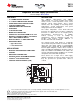
TMP512 TMP513 SBOS491A – JUNE 2010 – REVISED MAY 2011 www.ti.com Temperature and Power Supply System Monitors Check for Samples: TMP512, TMP513 FEATURES DESCRIPTION • • • • • • • • • • The TMP512 (dual-channel) and TMP513 (triple-channel) are system monitors that include remote sensors, a local temperature sensor, and a high-side current shunt monitor. These system monitors have the capability of measuring remote temperatures, on-chip temperatures, and system voltage/power/current consumption.
TMP512 TMP513 SBOS491A – JUNE 2010 – REVISED MAY 2011 www.ti.com This integrated circuit can be damaged by ESD. Texas Instruments recommends that all integrated circuits be handled with appropriate precautions. Failure to observe proper handling and installation procedures can cause damage. ESD damage can range from subtle performance degradation to complete device failure.
TMP512 TMP513 SBOS491A – JUNE 2010 – REVISED MAY 2011 www.ti.com THERMAL INFORMATION THERMAL METRIC TMP512 TMP512AIRSAR TMP512AIRSAT D (SOIC) RSA 14 16 (1) θJA Junction-to-ambient thermal resistance 91.1 34.3 θJC(top) Junction-to-case(top) thermal resistance 10.6 35.4 θJB Junction-to-board thermal resistance 40.3 11.6 ψJT Junction-to-top characterization parameter 49.1 0.5 ψJB Junction-to-board characterization parameter 47.5 11.
TMP512 TMP513 SBOS491A – JUNE 2010 – REVISED MAY 2011 www.ti.com ELECTRICAL CHARACTERISTICS: V+ = +12V Boldface limits apply over the specified temperature range, TA = –40°C to +125°C. At TA = +25°C, V+ = 12V, VSENSE = (VIN+ – VIN–) = 32mV, PGA = ÷ 1, and BRNG (1) = 1, unless otherwise noted.
TMP512 TMP513 SBOS491A – JUNE 2010 – REVISED MAY 2011 www.ti.com ELECTRICAL CHARACTERISTICS: V+ = +12V (continued) Boldface limits apply over the specified temperature range, TA = –40°C to +125°C. At TA = +25°C, V+ = 12V, VSENSE = (VIN+ – VIN–) = 32mV, PGA = ÷ 1, and BRNG(1) = 1, unless otherwise noted. TMP512, TMP513 PARAMETER TEST CONDITIONS MIN TYP MAX UNIT TEMPERATURE ERROR Local Temperature Sensor Remote Temperature Sensor (5) TELOCAL TEREMOTE vs Supply, Local TA = –40°C to +125°C ±1.
TMP512 TMP513 SBOS491A – JUNE 2010 – REVISED MAY 2011 www.ti.
TMP512 TMP513 SBOS491A – JUNE 2010 – REVISED MAY 2011 www.ti.
TMP512 TMP513 SBOS491A – JUNE 2010 – REVISED MAY 2011 www.ti.com TYPICAL CHARACTERISTICS: V+ = +12V At TA = +25°C, V+ = 12V, VSENSE = (VIN+ – VIN–) = 32mV, PGA = ÷ 1, and BRNG = 1, unless otherwise noted. FREQUENCY RESPONSE REMOTE TEMPERATURE ERROR vs TEMPERATURE 0 Remote Temperature Error (?C) -10 -20 Gain (dB) -30 -40 -50 -60 -70 -80 -90 -100 1k 100 10 10k 100k 6 5 4 3 2 1 0 -1 -2 -3 -4 -5 -6 34 Units Shown 0 -40 -25 1M 25 Figure 1.
TMP512 TMP513 SBOS491A – JUNE 2010 – REVISED MAY 2011 www.ti.com TYPICAL CHARACTERISTICS: V+ = +12V (continued) At TA = +25°C, V+ = 12V, VSENSE = (VIN+ – VIN–) = 32mV, PGA = ÷ 1, and BRNG = 1, unless otherwise noted. INTEGRAL NONLINEARITY vs INPUT VOLTAGE 20 200 15 10 150 32V Range 100 INL (mV) Gain Error (m%) BUS GAIN ERROR vs TEMPERATURE 250 50 5 0 -5 0 -10 16V Range -50 -15 -100 0 -40 -25 25 50 75 100 -20 -0.4 125 -0.2 -0.3 -0.1 0 0.1 0.2 0.3 0.
TMP512 TMP513 SBOS491A – JUNE 2010 – REVISED MAY 2011 www.ti.com TYPICAL CHARACTERISTICS: V+ = +12V (continued) At TA = +25°C, V+ = 12V, VSENSE = (VIN+ – VIN–) = 32mV, PGA = ÷ 1, and BRNG = 1, unless otherwise noted. ACTIVE IQ vs TWO-WIRE CLOCK FREQUENCY SHUTDOWN IQ vs TWO-WIRE CLOCK FREQUENCY 1100 250 V+ = 12V 1050 200 IQ (mA) IQ (mA) V+ = 12V V+ = 3.3V 1000 950 150 100 900 V+ = 3.3V 50 850 800 0 1k 10k 100k SCL Frequency (Hz) Figure 13.
TMP512 TMP513 SBOS491A – JUNE 2010 – REVISED MAY 2011 www.ti.com TYPICAL CHARACTERISTICS: V+ = +12V (continued) At TA = +25°C, V+ = 12V, VSENSE = (VIN+ – VIN–) = 32mV, PGA = ÷ 1, and BRNG = 1, unless otherwise noted. REMOTE TEMPERATURE ERROR vs SERIES RESISTANCE (GND Collector-Connected Transistor, 2N3906 PNP) 2.0 2.0 1.5 1.5 Remote Temperature Error (°C) Remote Temperature Error (°C) REMOTE TEMPERATURE ERROR vs SERIES RESISTANCE (Diode-Connected Transistor, 2N3906 PNP) 1.0 0.5 0 -0.5 -1.0 -1.
TMP512 TMP513 SBOS491A – JUNE 2010 – REVISED MAY 2011 www.ti.com PARAMETRIC MEASUREMENT INFORMATION TYPICAL CONNECTIONS Figure 18. SERIES RESISTANCE CONFIGURATION (a) GND Collector-Connected Transistor RS1 (1) DXP DXN RS2 (1) (b) Diode-Connected Transistor RS1 (1) DXP DXN RS2 (1) (1) RS1 + RS2 should be less than 1kΩ; see Filtering section. Figure 19. Figure 20.
TMP512 TMP513 SBOS491A – JUNE 2010 – REVISED MAY 2011 www.ti.com APPLICATION INFORMATION DESCRIPTION The TMP512/13 are digital temperature sensors with a digital current-shunt monitor that combine a local die temperature measurement channel and remote junction temperature measurement channels: two for the TMP512 and three for the TMP513. The TMP512/13 contain multiple registers for holding configuration information, temperature, and voltage measurement results.
TMP512 TMP513 SBOS491A – JUNE 2010 – REVISED MAY 2011 SERIES RESISTANCE CANCELLATION Series resistance in an application circuit that typically results from printed circuit board (PCB) trace resistance and remote line length is automatically cancelled by the TMP512/13, preventing what would otherwise result in a temperature offset. A total of up to 3kΩ of series line resistance is cancelled by the TMP512/13, eliminating the need for additional characterization and temperature offset correction.
TMP512 TMP513 SBOS491A – JUNE 2010 – REVISED MAY 2011 www.ti.com n-FACTOR CORRECTION REGISTER The TMP512/13 allow for a different n-factor value to be used for converting remote channel measurements to temperature. The remote channel uses sequential current excitation to extract a differential VBE voltage measurement to determine the temperature of the remote transistor. Equation 1 describes this voltage and temperature.
TMP512 TMP513 SBOS491A – JUNE 2010 – REVISED MAY 2011 www.ti.com Data transfer is then initiated and eight bits of data are sent, followed by an Acknowledge bit. During data transfer, SDA must remain stable while SCL is HIGH. Any change in SDA while SCL is HIGH is interpreted as a START or STOP condition. Once all data have been transferred, the master generates a STOP condition, indicated by pulling SDA from LOW to HIGH while SCL is HIGH.
TMP512 TMP513 SBOS491A – JUNE 2010 – REVISED MAY 2011 www.ti.
TMP512 TMP513 SBOS491A – JUNE 2010 – REVISED MAY 2011 www.ti.com ALERT 1 9 1 9 SCL SDA 0 0 0 1 1 0 0 1 R/W Start By Master 0 1 1 ACK By TMP512/TMP513 1 A1 A0 0 From NACK By TMP512/TMP513 Master Frame 1 SMBus ALERT Response Address Byte Frame 2 Slave Address Byte Stop By Master (1) NOTE (1): The value of the Slave Address Byte is determined by the settings of the A0 pin. Refer to Table 1. Figure 26.
TMP512 TMP513 SBOS491A – JUNE 2010 – REVISED MAY 2011 www.ti.com TIMING DIAGRAMS Figure 28 describes the timing operations on the TMP512/13. Parameters for Figure 28 are defined in Table 2. Bus definitions are: Bus Idle: Both SDA and SCL lines remain high. Start Data Transfer: A change in the state of the SDA line, from high to low, while the SCL line is high, defines a START condition. Each data transfer initiates with a START condition. Denoted as S in Figure 28.
TMP512 TMP513 SBOS491A – JUNE 2010 – REVISED MAY 2011 www.ti.com HIGH-SPEED MODE SENSOR FAULT In order for the two-wire bus to operate at frequencies above 400kHz, the master device must issue a High-Speed mode (Hs-mode) master code (0000 1xxx) as the first byte after a START condition to switch the bus to high-speed operation. The TMP512/13 do not acknowledge this byte, but switch the input filters on SDA and SCL and the output filter on SDA to operate in Hs-mode, allowing transfers at up to 3.4MHz.
TMP512 TMP513 SBOS491A – JUNE 2010 – REVISED MAY 2011 www.ti.com The TMP512/13 support reset via the two-wire General Call address 00h (0000 0000b). The TMP512/13 acknowledge the General Call address and respond to the second byte. If the second byte is 06h (0000 0110b), the TMP512/13 execute a software reset state to all TMP512/13 registers, and abort any conversion in progress. The TMP512/13 take no action in response to other values in the second byte.
TMP512 TMP513 SBOS491A – JUNE 2010 – REVISED MAY 2011 www.ti.com TMP512 TMP513 MUX DXP1 Low-Pass Filter DXN1 ADC DXP2 DXN2 DXP3 Internal Diode Temperature Sensor DXN3 V+ Subregulator 3.3V Filter C 3.3V Supply ´ VSHUNT = VIN+ - VINTypically < 50mV VIN- Two-Wire Interface Current Register VIN+ Current Shunt A0 Power Register ADC ALERT SDA SMBus Controller SCL Voltage Register Load GPIO VBUS = VIN- - GND Range of 0V to 26V Typical Application: 12V GND Figure 29.
TMP512 TMP513 SBOS491A – JUNE 2010 – REVISED MAY 2011 www.ti.com COMPATIBILITY WITH TI HOT-SWAP CONTROLLERS The TMP512/13 are designed for compatibility with hot-swap controllers such the TI TPS2490. The TPS2490 uses a high-side shunt with a limit at 50mV; the TMP512/13 full-scale range of 40mV enables the use of the same shunt for current sensing below this limit.
TMP512 TMP513 SBOS491A – JUNE 2010 – REVISED MAY 2011 www.ti.com In applications that do not have large energy storage electrolytics on one or both sides of the shunt, an input overstress condition may result from an excessive dV/dt of the voltage applied to the input. A hard physical short is the most likely cause of this event, particularly in applications with no large electrolytics present.
TMP512 TMP513 SBOS491A – JUNE 2010 – REVISED MAY 2011 www.ti.com TMP512 TMP513 MUX DXP1 Low-Pass Filter DXN1 ADC DXP2 DXN2 DXP3 Internal Diode Temperature Sensor DXN3 V+ Subregulator 3.3V Filter C 3.
TMP512 TMP513 SBOS491A – JUNE 2010 – REVISED MAY 2011 www.ti.com PROGRAMMING THE TMP512/13 POWER MEASUREMENT ENGINE Calibration Register and Scaling The Calibration Register makes it possible to set the scaling of the Current and Power Registers to whatever values are most useful for a given application.
TMP512 TMP513 SBOS491A – JUNE 2010 – REVISED MAY 2011 www.ti.com 6. Calculate the Power LSB with Equation 10. Equation 10 shows a general formula; because the bus voltage measurement LSB is always 4mV, the power formula reduces to the calculated result. Power_LSB = 20 Current_LSB Power_LSB = 400 ´ 10-6 (10) 7. Compute the maximum current and shunt voltage values (before overflow), as shown by Equation 11 and Equation 12.
TMP512 TMP513 SBOS491A – JUNE 2010 – REVISED MAY 2011 www.ti.com Figure 32.
TMP512 TMP513 SBOS491A – JUNE 2010 – REVISED MAY 2011 www.ti.com Calibration Example 2 (Overflow Possible) This design example uses the nine-step procedure for calibrating the TMP512/13 where overflow is possible. Figure 33 illustrates how the same procedure is performed using the automated TMP512/13EVN software. The same numbers used in the nine-step example are used in the software example shown in Figure 33.
TMP512 TMP513 SBOS491A – JUNE 2010 – REVISED MAY 2011 www.ti.com 7. Compute the maximum current and shunt voltage values (before overflow), as shown by Equation 20 and Equation 21. Note that both Equation 20 and Equation 21 involve an If - then condition. Max_Current = Current_LSB ´ 32767 Max_Current = 0.
TMP512 TMP513 www.ti.com SBOS491A – JUNE 2010 – REVISED MAY 2011 Figure 33.
TMP512 TMP513 SBOS491A – JUNE 2010 – REVISED MAY 2011 www.ti.com REGISTER INFORMATION The TMP512/13 uses a bank of registers for holding configuration settings, measurement results, maximum/minimum limits, and status information. Table 3 summarizes the TMP512/13 registers. Register contents are updated 4μs after completion of the write command.
TMP512 TMP513 SBOS491A – JUNE 2010 – REVISED MAY 2011 www.ti.com Table 3. Summary of Register Set (continued) POINTER ADDRESS POWER-ON RESET BINARY HEX TYPE (1) Contains positive limit for remote temperature. 00101010 10000000 2A80 R/W Remote Temperature Limit 2 Contains positive limit for remote temperature. 00101010 10000000 2A80 R/W 14 (4) Remote Temperature Limit 3 Contains positive limit for remote temperature.
TMP512 TMP513 SBOS491A – JUNE 2010 – REVISED MAY 2011 www.ti.com Table 4. PG Bit Settings (1) (1) PG1 PG0 GAIN RANGE 0 0 1 ±40mV 0 1 ÷2 ±80mV 1 0 ÷4 ±160mV 1 1 ÷8 ±320mV Shaded values are default. BADC: BADC Bus ADC Resolution/Averaging Bits 10–7 These bits adjust the Bus ADC resolution (9-, 10-, 11-, or 12-bit) or set the number of samples used when averaging results for the Bus Voltage Register (05h).
TMP512 TMP513 SBOS491A – JUNE 2010 – REVISED MAY 2011 www.ti.
TMP512 TMP513 SBOS491A – JUNE 2010 – REVISED MAY 2011 • • • www.ti.com When all of the following conditions are met, the temperature sensor core triggers a single conversion of the voltage measurement core at the same rate as the conversion rate shown by bits R2 to R0. The conversion rate is different than '111'; There is at least one enabled temperature channel; and The voltage measurement core is in triggered mode of operation.
TMP512 TMP513 SBOS491A – JUNE 2010 – REVISED MAY 2011 www.ti.com Status Register 02h (Read) BIT # D15 D14 D13 D12 D11 D10 D9 D8 D7 D6 D5 D4 D3 D2 D1 D0 BIT NAME SHP SHN BVP BVN PWR LCL RM1 RM2 RM3 CVR CRT PVLD SMBA OVF — — POR VALUE 0 0 0 0 0 0 0 0 0 0 0 0 0 0 0 0 The Status Register flags activate whenever any limit is violated, and latch if the alert is in latch mode.
TMP512 TMP513 SBOS491A – JUNE 2010 – REVISED MAY 2011 www.ti.com Bit Descriptions (continued) RM3: Remote Temperature 3 Over-Limit (TMP513 only) Bit 7 This bit is set to '1' when the result in the Remote Temperature Result 3 Register (0Bh) exceeds the level set in the Remote Temperature Limit 3 Register (14h) plus half of the temperature hysteresis. It sets also if during conversion of remote channel 3 an open diode condition was detected.
TMP512 TMP513 SBOS491A – JUNE 2010 – REVISED MAY 2011 www.ti.
TMP512 TMP513 SBOS491A – JUNE 2010 – REVISED MAY 2011 www.ti.com Bit Descriptions (continued) FC0, FC1 Fault Count Control Bits The Fault Count Control Bits affect flags in SMBus Alert Register bits D15-D7. Bit 3, 2 00: These flags are activated after the first conversion result with a violated limit. 01: These flags are activated after the second consecutive conversion result with a violated limit. 10: These flags are activated after the fourth consecutive conversion result with a violated limit.
TMP512 TMP513 SBOS491A – JUNE 2010 – REVISED MAY 2011 www.ti.com Shunt Voltage Register 04h (Read-Only) The Shunt Voltage Register stores the current shunt voltage reading, VSHUNT. Shunt Voltage Register bits are shifted according to the PGA setting selected in Configuration Register 1 (00h). When multiple sign bits are present, they will all be the same value. Negative numbers are represented in twos complement format.
TMP512 TMP513 SBOS491A – JUNE 2010 – REVISED MAY 2011 www.ti.com Table 9. Shunt Voltage Register Format (1) VSHUNT Reading (mV) Decimal Value PGA = ÷ 8 (D15…..................D0) PGA = ÷ 4 (D15…..................D0) PGA = ÷ 2 (D15…..................D0) PGA = ÷ 1 (D15…..................D0) 320.02 32002 0111 1101 0000 0000 0011 1110 1000 0000 0001 1111 0100 0000 0000 1111 1010 0000 320.01 32001 0111 1101 0000 0000 0011 1110 1000 0000 0001 1111 0100 0000 0000 1111 1010 0000 320.
TMP512 TMP513 SBOS491A – JUNE 2010 – REVISED MAY 2011 www.ti.com Bus Voltage Register 05h (Read-Only) The Bus Voltage Register stores the most recent bus voltage reading, VBUS. At full-scale range = 32V (decimal = 8000, hex = 1F40), and LSB = 4mV.
TMP512 TMP513 SBOS491A – JUNE 2010 – REVISED MAY 2011 www.ti.com Local Temperature Result Register 08h (Read-Only) BIT # D15 D14 D13 D12 D11 D10 D9 D8 D7 D6 D5 D4 D3 D2 D1 D0 BIT NAME T12 T11 T10 T9 T8 T7 T6 T5 T4 T3 T2 T1 T0 — PVLD — POR VALUE 0 0 0 0 0 0 0 0 0 0 0 0 0 0 0 0 The data format is 13 bits, 0.0625°C per bit. Full-scale allows display up to ±256°C.
TMP512 TMP513 SBOS491A – JUNE 2010 – REVISED MAY 2011 www.ti.com Remote Temperature Result 1 Register 09h, Remote Temperature Result 2 Register 0Ah, Remote Temperature Result 3 Register (TMP513 Only) 0Bh (Read-Only) BIT # D15 D14 D13 D12 D11 D10 D9 D8 D7 D6 D5 D4 D3 D2 D1 D0 BIT NAME RT12 RT11 RT10 RT9 RT8 RT7 RT6 RT5 RT4 RT3 RT2 RT1 RT0 — PVLD DO POR VALUE 0 0 0 0 0 0 0 0 0 0 0 0 0 0 0 0 The data format is 13 bits, 0.0625°C per bit.
TMP512 TMP513 SBOS491A – JUNE 2010 – REVISED MAY 2011 www.ti.com Bus Voltage Negative Limit Register 0Fh (Read/Write) At full-scale range = 32V (decimal = 8000, hex = 1F40), and LSB = 4mV.
TMP512 TMP513 SBOS491A – JUNE 2010 – REVISED MAY 2011 www.ti.com n-Factor 1 Register 16h (Read/Write) BIT # D15 D14 D13 D12 D11 D10 D9 D8 D7 D6 D5 D4 D3 D2 D1 D0 BIT NAME NF7 NF6 NF5 NF4 NF3 NF2 NF1 NF0 HST7 HST6 HST5 HST4 HST3 HST2 HST1 HST0 POR VALUE 0 0 0 0 0 0 0 0 0 0 0 0 0 0 0 0 NF7–NF0: n-Factor Bits Bits 15-8 Shows the n-factor for Channel 1 according to the range indicated in Table 11. Table 11.
TMP512 TMP513 SBOS491A – JUNE 2010 – REVISED MAY 2011 www.ti.com Manufacturer ID Register 1Eh and FEh (Read-Only) BIT # D15 D14 D13 D12 D11 D10 D9 D8 D7 D6 D5 D4 D3 D2 D1 D0 BIT NAME ID7 ID6 ID5 ID4 ID3 ID2 ID1 ID0 — — — — — — — — POR VALUE 0 1 0 1 0 1 0 1 1 1 1 1 1 1 1 1 ID7–ID0: Identification Register Bits Bits 15-8 These bits provide the manufacturer ID.
TMP512 TMP513 SBOS491A – JUNE 2010 – REVISED MAY 2011 www.ti.com REVISION HISTORY NOTE: Page numbers for previous revisions may differ from page numbers in the current version. Changes from Original (June, 2010) to Revision A Page • Removed product preview indications for QFN-16 package option of TMP513 throughout document ............................... 1 • Added package information for QFN-16 version of TMP512 .........................................................................................
PACKAGE OPTION ADDENDUM www.ti.
PACKAGE OPTION ADDENDUM www.ti.com 11-Apr-2013 (4) Multiple Top-Side Markings will be inside parentheses. Only one Top-Side Marking contained in parentheses and separated by a "~" will appear on a device. If a line is indented then it is a continuation of the previous line and the two combined represent the entire Top-Side Marking for that device. Important Information and Disclaimer:The information provided on this page represents TI's knowledge and belief as of the date that it is provided.
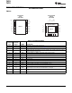
PACKAGE MATERIALS INFORMATION www.ti.com 26-Jan-2013 TAPE AND REEL INFORMATION *All dimensions are nominal Device Package Package Pins Type Drawing SPQ Reel Reel A0 Diameter Width (mm) (mm) W1 (mm) B0 (mm) K0 (mm) P1 (mm) W Pin1 (mm) Quadrant TMP512AIDR SOIC D 14 2500 330.0 16.4 6.5 9.0 2.1 8.0 16.0 Q1 TMP512AIRSAR QFN RSA 16 3000 330.0 12.4 4.25 4.25 1.15 8.0 12.0 Q2 TMP512AIRSAT QFN RSA 16 250 180.0 12.4 4.25 4.25 1.15 8.0 12.
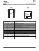
PACKAGE MATERIALS INFORMATION www.ti.com 26-Jan-2013 *All dimensions are nominal Device Package Type Package Drawing Pins SPQ Length (mm) Width (mm) Height (mm) TMP512AIDR TMP512AIRSAR SOIC D 14 2500 367.0 367.0 38.0 QFN RSA 16 3000 367.0 367.0 35.0 TMP512AIRSAT QFN RSA 16 250 210.0 185.0 35.0 TMP513AIDR SOIC D 16 2500 367.0 367.0 38.0 TMP513AIRSAR QFN RSA 16 3000 367.0 367.0 35.0 TMP513AIRSAT QFN RSA 16 250 210.0 185.0 35.
IMPORTANT NOTICE Texas Instruments Incorporated and its subsidiaries (TI) reserve the right to make corrections, enhancements, improvements and other changes to its semiconductor products and services per JESD46, latest issue, and to discontinue any product or service per JESD48, latest issue. Buyers should obtain the latest relevant information before placing orders and should verify that such information is current and complete.