
Datasheet


Configuration 1 Configuration 2 Configuration 3
GND
ADC
Subregulator
3.3V
Subregulator
3.3V
V+ = 4.5V to 26V
Filter C
Load
470nF
Bus Voltage Range = 4.5V to 26V
Shunt
R
SHUNT
V
IN+
V
IN-
GND
ADC
V+ = 4.5V to 26V
Load
Filter C
470nF
Bus Voltage Range = 0V to 26V
Shunt
R
SHUNT
V
IN+
V
IN-
GND
ADC
Subregulator
3.3V
V+ = 3V to 5.5V
Load
Filter C
100nF
Bus Voltage Range = 0V to 26V
Shunt
R
SHUNT
V
IN+
V
IN-
TMP512
TMP513
www.ti.com
SBOS491A –JUNE 2010– REVISED MAY 2011
APPLICATION INFORMATION
between the two systems is being addressed. Two
bi-directional lines, SCL and SDA, connect the
DESCRIPTION
TMP512/13 to the bus. SDA is an open-drain
The TMP512/13 are digital temperature sensors with
connection. See Figure 23 for a typical application
a digital current-shunt monitor that combine a local
circuit.
die temperature measurement channel and remote
junction temperature measurement channels: two for
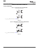
SUBREGULATOR
the TMP512 and three for the TMP513. The
TMP512/13 contain multiple registers for holding The subregulator can be configured to three different
configuration information, temperature, and voltage modes of operation. Each mode has its advantage
measurement results. These devices provide digital and limitation. Figure 22 shows the three
current, voltage, and power readings necessary for configuration arrangements. The minimum
accurate decision-making in precisely-controlled capacitance on the Filter C pin for Configurations 1
systems. Programmable registers allow flexible and 2 is 470nF. The minimum capacitance on the
configuration for setting warning limits, measurement Filter C pin for Configuration 3 is 100nF.
resolution, and continuous-versus-triggered
Configuration 1 has V+ and V
IN+
tied together. V+
operation. Detailed register information appears at
supplies the subregulator, which in turn supplies the
the end of this data sheet, beginning with Table 3.
3.3V to the Filter C pin and the internal die. With the
For proper remote temperature sensing operation, the V+ supply range of 4.5V to 26V connected to the
TMP512 requires transistors connected between shunt voltage, the bus voltage range cannot go to
DXP1 and DXN1 and between DXP2 and DXN2, and zero and is limited to 4.5V to 26V.
for the TMP513, between DXP3 and DXN3 as well.
Configuration 2 has V+ to the subregulator without
Unused channels on the TMP512/13 must be
any other connections. Under this configuration, the
connected to GND.
bus voltage range can go from 0V to 26V, because it
The TMP512/13 offer compatibility with two-wire and is not limited to 4.5V as in Configuration 1.
SMBus interfaces. The two-wire and SMBus
Configuration 3 has the subregulator V+ and Filter C
protocols are essentially compatible with each other.
pins shorted together. V+ is limited to 3V to 5.5V
Two-wire is used throughout this data sheet, with
because the Filter C pin supplies the internal die; it
SMBus being specified only when a difference
cannot exceed this voltage range. The bus voltage
range can go from 0V to 26V, because it is not limited
to 4.5V as in Configuration 1.
Figure 22. Typical Subregulator Configurations
Copyright © 2010–2011, Texas Instruments Incorporated 13