
Datasheet

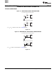


V V =-
BE2 BE1
nkT
q
I
I
2
1
(
(
In
n =
eff
1.008 300
(300 N )-
ADJUST
´
N 300
ADJUST
-=
300 1.008
n
eff
´
(
(
´
Power Register
Current Register
Two-Wire
Interface
Voltage Register
ADC
GND
GPIO
DXP1
DXN1
DXP2
DXN2
ADC
Low-Pass Filter
MUX
DXP3
DXN3
V
IN+
V
IN-
Current
Shunt
Load
Filter C
V+
Subregulator
3.3V
Internal
Diode
Temperature
Sensor
A0
ALERT
SDA
SCL
SMBus
Controller
3.3V Supply
TMP512
TMP513
TMP512
TMP513
www.ti.com
SBOS491A –JUNE 2010– REVISED MAY 2011
n-FACTOR CORRECTION REGISTER twos-complement format, yielding an effective data
range from –128 to +127. The n-factor value may be
The TMP512/13 allow for a different n-factor value to
written to and read from pointer address 16h for
be used for converting remote channel
remote channel 1, pointer address 17h for remote
measurements to temperature. The remote channel
channel 2, and pointer address 18h for remote
uses sequential current excitation to extract a
channel 3. The register power-on reset value is 00h,
differential V
BE
voltage measurement to determine
thus having no effect unless the register is written to.
the temperature of the remote transistor. Equation 1
describes this voltage and temperature.
BUS OVERVIEW
The device that initiates the transfer is called a
(1)
master, and the devices controlled by the master are
slaves. The bus must be controlled by a master
The value n in Equation 1 is a characteristic of the
device that generates the serial clock (SCL), controls
particular transistor used for the remote channel. The
the bus access, and generates START and STOP
power-on reset value for the TMP512/13 is n = 1.008.
conditions.
The value in the n-Factor Correction Register may be
used to adjust the effective n-factor according to
To address a specific device, the master initiates a
Equation 2 and Equation 3.
START condition by pulling the data signal line (SDA)
from a HIGH to a LOW logic level while SCL is HIGH.
All slaves on the bus shift in the slave address byte
(2)
on the rising edge of SCL, with the last bit indicating
whether a read or write operation is intended. During
the ninth clock pulse, the slave being addressed
(3)
responds to the master by generating an
The n-factor value must be stored in Acknowledge and pulling SDA LOW.
Figure 23. Typical Application Circuit
Copyright © 2010–2011, Texas Instruments Incorporated 15