
Datasheet


TMP512
TMP513
SBOS491A –JUNE 2010– REVISED MAY 2011
www.ti.com
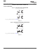
Data transfer is then initiated and eight bits of data WRITING TO/READING FROM THE
are sent, followed by an Acknowledge bit. During TMP512/13
data transfer, SDA must remain stable while SCL is
Accessing a particular register on the TMP512/13 is
HIGH. Any change in SDA while SCL is HIGH is
accomplished by writing the appropriate value to the
interpreted as a START or STOP condition.
register pointer. Refer to Table 3 for a complete list of
Once all data have been transferred, the master registers and corresponding addresses. The value for
generates a STOP condition, indicated by pulling the register pointer as shown in Figure 26 is the first
SDA from LOW to HIGH while SCL is HIGH. The byte transferred after the slave address byte with the
TMP512/13 includes a 28ms timeout on its interface R/W bit LOW. Every write operation to the
to prevent locking up an SMBus. TMP512/13 requires a value for the register pointer.
Writing to a register begins with the first byte
SERIAL BUS ADDRESS
transmitted by the master. This byte is the slave
address, with the R/W bit LOW. The TMP512/13 then
To communicate with the TMP512/13, the master
acknowledge receipt of a valid address. The next
must first address slave devices via a slave address
byte transmitted by the master is the address of the
byte. The slave address byte consists of seven
register to which data will be written. This register
address bits, and a direction bit indicating the intent
address value updates the register pointer to the
of executing a read or write operation.
desired register. The next two bytes are written to the
The TMP512/13 feature an address pin to allow up to
register addressed by the register pointer. The
four devices to be addressed on a single bus. Table 1
TMP512/13 acknowledge receipt of each data byte.
describes the pin logic levels used to properly
The master may terminate data transfer by
connect up to four devices. The state of the A0 pin is
generating a START or STOP condition.
sampled on every bus communication and should be
When reading from the TMP512/13, the last value
set before any activity on the interface occurs. The
stored in the register pointer by a write operation
address pin is read at the start of each
determines which register is read during a read
communication event.
operation. To change the register pointer for a read
operation, a new value must be written to the register
Table 1. TMP512/13 Address Pins and
Slave Addresses pointer. This write is accomplished by issuing a slave
address byte with the R/W bit LOW, followed by the
DEVICE TWO-WIRE
register pointer byte. No additional data are required.
ADDRESS A0 PIN CONNECTION
The master then generates a START condition and
1011100 Ground
sends the slave address byte with the R/W bit HIGH
1011101 V+
to initiate the read command. The next byte is
1011110 SDA
transmitted by the slave and is the most significant
byte of the register indicated by the register pointer.
1011111 SCL
This byte is followed by an Acknowledge from the
master; then the slave transmits the least significant
SERIAL INTERFACE
byte. The master acknowledges receipt of the data
The TMP512/13 operate only as slave devices on the byte. The master may terminate data transfer by
two-wire bus and SMBus. SCL is an input only, and generating a Not-Acknowledge after receiving any
TMP512/13 cannot drive it. Connections to the bus data byte, or generating a START or STOP condition.
are made via the open-drain I/O lines SDA and SCL. If repeated reads from the same register are desired,
The SDA and SCL pins feature integrated spike it is not necessary to continually send the register
suppression filters and Schmitt triggers to minimize pointer bytes; the TMP512/13 retain the register
the effects of input spikes and bus noise. The pointer value until it is changed by the next write
TMP512/13 support the transmission protocol for fast operation.
(1kHz to 400kHz) and high-speed (1kHz to 3.4MHz)
Figure 24 and Figure 25 show read and write
modes. All data bytes are transmitted MSB first.
operation timing diagrams, respectively. Note that
register bytes are sent most-significant byte first,
followed by the least significant byte. See Figure 27
for an illustration of a typical register pointer
configuration.
16 Copyright © 2010–2011, Texas Instruments Incorporated