
Datasheet

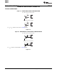


Frame1Two-WireSlaveAddressByte
(1)
Frame2DataMSByte
(2)
1
StartBy
Master
ACKBy
TMP512/TMP513
ACKBy
Master
From
TMP512/TMP513
1 9 1
9
SDA
SCL
0 1 1 R/
W D15 D14 D13 D12 D11 D10 D9 D8
1 A1 A0
Frame3DataLSByte
(2)
StopNoACKBy
(3)
Master
From
TMP512/TMP513
1
9
D7 D6 D5 D4 D3 D2 D1 D0
NOTES:(1)ThevalueoftheSlaveAddressByteisdeterminedbythesettingsoftheA0pin.
RefertoTable1.
(2)Readdataisfromthelastregisterpointerlocation.Ifanewregisterisdesired,theregister
pointermustbeupdated.SeeFigure23.
(3)ACKbyMastercanalsobesent.
Frame1Two-WireSlaveAddressByte
(1)
Frame2RegisterPointerByte
StartBy
Master
ACKBy
TMP512/TMP513
ACKBy
TMP512/TMP513
1 9 1
ACKBy
TMP512/TMP513
1
D15 D14 D13 D12 D11 D10 D9 D8
9
9
SDA
SCL
1 0 1 1 1
A1 A0 R/W P7 P6 P5 P4 P3 P2 P1 P0
NOTE(1):ThevalueoftheSlaveAddressByteisdeterminedbythesettingsoftheA0pin.RefertoTable1.
Frame4DataLSByteFrame3DataMSByte
ACKBy
TMP512/TMP513
StopBy
Master
1
D7 D6 D5 D4 D3 D2 D1 D0
9
TMP512
TMP513
www.ti.com
SBOS491A –JUNE 2010– REVISED MAY 2011
Figure 25. Timing Diagram for Read Word Format
Figure 24. Timing Diagram for Write Word Format
Copyright © 2010–2011, Texas Instruments Incorporated 17