
Datasheet


SCL
SDA
t
(LOW)
t
R
t
F
t
(HDSTA)
t
(HDSTA)
t
(HDDAT)
t
(BUF)
t
(SUDAT)
t
(HIGH)
t
(SUSTA)
t
(SUSTO)
P S S P
TMP512
TMP513
www.ti.com
SBOS491A –JUNE 2010– REVISED MAY 2011
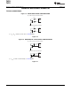
TIMING DIAGRAMS Data Transfer: The number of data bytes transferred
between a START and a STOP condition is not
Figure 28 describes the timing operations on the
limited and is determined by the master device. The
TMP512/13. Parameters for Figure 28 are defined in
receiver acknowledges data transfer.
Table 2. Bus definitions are:
Acknowledge: Each receiving device, when
Bus Idle: Both SDA and SCL lines remain high.
addressed, is obliged to generate an Acknowledge
bit. A device that acknowledges must pull down the
Start Data Transfer: A change in the state of the
SDA line during the Acknowledge clock pulse in such
SDA line, from high to low, while the SCL line is high,
a way that the SDA line is stable low during the high
defines a START condition. Each data transfer
period of the Acknowledge clock pulse. Setup and
initiates with a START condition. Denoted as S in
hold times must be taken into account. On a master
Figure 28.
receive, data transfer termination can be signaled by
Stop Data Transfer: A change in the state of the
the master generating a Not-Acknowledge on the last
SDA line from low to high while the SCL line is high
byte that has been transmitted by the slave.
defines a STOP condition. Each data transfer
terminates with a repeated START or STOP
condition. Denoted as P in Figure 28.
Figure 28. Two-Wire Timing Diagram
Table 2. Timing Characteristics for Figure 28
FAST MODE HIGH-SPEED MODE
PARAMETER MIN MAX MIN MAX UNIT
SCL Operating Frequency f
(SCL)
0.001 0.4 0.001 3.4 MHz
Bus Free Time Between STOP and START Condition t
(BUF)
600 160 ns
Hold time after repeated START condition. After this period, the first clock
t
(HDSTA)
100 100 ns
is generated.
Repeated START Condition Setup Time t
(SUSTA)
100 100 ns
STOP Condition Setup Time t
(SUSTO)
100 100 ns
Data Hold Time t
(HDDAT)
0
(1)
0
(2)
ns
Data Setup Time t
(SUDAT)
100 10 ns
SCL Clock LOW Period t
(LOW)
1300 160 ns
SCL Clock HIGH Period t
(HIGH)
600 60 ns
Clock/Data Fall Time t
F
300 160 ns
Clock/Data Rise Time t
R
300 160
ns
for SCL ≤ 100kHz t
R
1000
(1) For cases with fall time of SCL less than 20ns and/or the rise or fall time of SDA less than 20ns, the hold time should be greater than
20ns.
(2) For cases with a fall time of SCL less than 10ns and/or the rise or fall time of SDA less than 10ns, the hold time should be greater than
10ns.
Copyright © 2010–2011, Texas Instruments Incorporated 19