
Datasheet
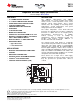

TMP512
TMP513
SBOS491A –JUNE 2010– REVISED MAY 2011
www.ti.com
This integrated circuit can be damaged by ESD. Texas Instruments recommends that all integrated circuits be handled with
appropriate precautions. Failure to observe proper handling and installation procedures can cause damage.
ESD damage can range from subtle performance degradation to complete device failure. Precision integrated circuits may be more
susceptible to damage because very small parametric changes could cause the device not to meet its published specifications.
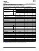
PACKAGE INFORMATION
(1)
PRODUCT PACKAGE-LEAD PACKAGE DESIGNATOR PACKAGE MARKING
SO-14 D TMP512A
TMP512
QFN-16 RSA TMP512A
SO-16 D TMP513A
TMP513
QFN-16 RSA TMP513A
(1) For the most current package and ordering information see the Package Option Addendum at the end of this document, or visit the
TMP512/TMP513 product folder at www.ti.com.
ABSOLUTE MAXIMUM RATINGS
(1)
Over operating free-air temperature range (unless otherwise noted).
TMP512, TMP513 UNIT
Supply Voltage, V+ 26 V
Voltage GND – 0.3 to +6 V
Filter C
Current 10 mA
Differential (V
IN+
) – (V
IN–
)
(2)
–26 to +26 V
Analog Inputs, V
IN+
, V
IN–
Common-Mode –0.3 to +26 V
Open-Drain Digital Outputs GND – 0.3 to +6 V
GPIO, DXP, DXN GND – 0.3 to V+ + 0.3 V
Input Current Into Any Pin 5 mA
Open-Drain Digital Output Current 10 mA
Storage Temperature –65 to +150 °C
Junction Temperature +150 °C
Human Body Model (HBM) 2000 V
ESD Ratings Charged-Device Model (CDM) 1000 V
Machine Model (MM) 150 V
(1) Stresses above these ratings may cause permanent damage. Exposure to absolute maximum conditions for extended periods may
degrade device reliability. These are stress ratings only, and functional operation of the device at these or any other conditions beyond
those specified is not implied.
(2) V
IN+
and V
IN–
may have a differential voltage of –26V to +26V; however, the voltage at these pins must not exceed the range –0.3V to
+26V.
2 Copyright © 2010–2011, Texas Instruments Incorporated