
Datasheet


TMP512
TMP513
SBOS491A –JUNE 2010– REVISED MAY 2011
www.ti.com
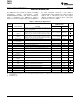
Table 4. PG Bit Settings
(1)
PG1 PG0 GAIN RANGE
0 0 1 ±40mV
0 1 ÷2 ±80mV
1 0 ÷4 ±160mV
1 1 ÷8 ±320mV
(1) Shaded values are default.
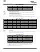
BADC: BADC Bus ADC Resolution/Averaging
Bits 10–7 These bits adjust the Bus ADC resolution (9-, 10-, 11-, or 12-bit) or set the number of samples used when
averaging results for the Bus Voltage Register (05h).
SADC: SADC Shunt ADC Resolution/Averaging
Bits 6–3 These bits adjust the Shunt ADC resolution (9-, 10-, 11-, or 12-bit) or set the number of samples used when
averaging results for the Shunt Voltage Register (04h).
BADC (Bus) and SADC (Shunt) ADC resolution/averaging and conversion time settings are shown in Table 5.
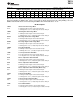
Table 5. ADC Settings
(1)
ADC4 ADC3 ADC2 ADC1 MODE/SAMPLES CONVERSION TIME
0 X
(2)
0 0 9-bit 105μs
0 X
(2)
0 1 10-bit 185μs
0 X
(2)
1 0 11-bit 345μs
0 X
(2)
1 1 12-bit 665μs
1 0 0 0 12-bit 665μs
1 0 0 1 2 1.3ms
1 0 1 0 4 2.58ms
1 0 1 1 8 5.13ms
1 1 0 0 16 10.25ms
1 1 0 1 32 20.49ms
1 1 1 0 64 40.97ms
1 1 1 1 128 81.92ms
(1) Shaded values are default.
(2) X = Don't care.
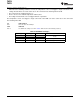
MODE: Operating Mode
Bits 2–0 Selects continuous, triggered, or power-down mode of operation. These bits default to continuous shunt and bus
measurement mode. The mode settings are shown in Table 6.
Table 6. Mode Settings
(1)
MODE3 MODE2 MODE1 MODE
0 0 0 Power-Down
(2)
0 0 1 Shunt Voltage, Triggered
(3)
0 1 0 Bus Voltage, Triggered
(3)
0 1 1 Shunt and Bus, Triggered
(3)
1 0 0 ADC Off (disabled)
(4)
1 0 1 Shunt Voltage, Continuous
1 1 0 Bus Voltage, Continuous
1 1 1 Shunt and Bus, Continuous
(1) Shaded values are default.
(2) Combination '000' stops converter immediately.
(3) In triggered modes the converter goes to power down. It can be triggered by a write of '1' to bit 14
(One-Shot) in Configuration Register 1 or by the delay scheme of the temperature sensor core. See
Table 7.
(4) Combination '100' stops the converter at conversion end.
34 Copyright © 2010–2011, Texas Instruments Incorporated