
Datasheet

TMP512
TMP513
SBOS491A –JUNE 2010– REVISED MAY 2011
www.ti.com
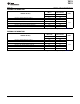
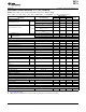
ELECTRICAL CHARACTERISTICS: V+ = +12V
Boldface limits apply over the specified temperature range, T
A
= –40°C to +125°C.
At T
A
= +25°C, V+ = 12V, V
SENSE
= (V
IN+
– V
IN–
) = 32mV, PGA = ÷ 1, and BRNG
(1)
= 1, unless otherwise noted.
TMP512, TMP513
PARAMETER TEST CONDITIONS MIN TYP MAX UNIT
INPUT
Current Sense (Input) Voltage Range PGA = ÷ 1 0 ±40 mV
PGA = ÷ 2 0 ±80 mV
PGA = ÷ 4 0 ±160 mV
PGA = ÷ 8 0 ±320 mV
Bus Voltage (Input Voltage) Range
(2)
BRNG = 0 0 16 V
BRNG = 1 0 32 V
Common-Mode Rejection CMRR V
IN+
= 0V to 26V 100 120 dB
Offset Voltage, RTI
(3)
V
OS
PGA = ÷ 1 ±10 ±100 μV
PGA = ÷ 2 ±20 ±125 μV
PGA = ÷ 4 ±30 ±150 μV
PGA = ÷ 8 ±40 ±200 μV
vs Temperature 0.2 μV/°C
V+ = 3V to 5.5V, Configuration 3
(4)
10 μV/V
vs Power Supply PSRR
V+ = 4.5V to 26V, subregulator supply 0.1 μV/V
Current Sense Gain Error ±0.04 %
vs Temperature 0.0025 %
Input Impedance Active Mode
V
IN+
Pin 20 μA
V
IN–
Pin 20 || 320 μA || kΩ
Input Leakage Power-Down Mode
V
IN+
Pin 0.1 0.5 μA
V
IN–
Pin 0.1 0.5 μA
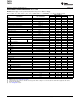
DC ACCURACY
ADC Basic Resolution 12 Bits
1 LSB Step Size
Shunt Voltage 10 μV
Bus Voltage 4 mV
Current Measurement Error ±0.2 ±0.5 %
over Temperature ±1 %
Bus Voltage Measurement Error ±0.2 ±0.5 %
over Temperature ±1 %
Differential Nonlinearity ±0.1 LSB
ADC TIMING
ADC Conversion Time 12-Bit 665 733 μs
11-Bit 345 380 μs
10-Bit 185 204 μs
9-Bit 105 117 μs
(1) BRNG is bit 13 of Configuration Register 1.
(2) This parameter only expresses the full-scale range of the ADC scaling. In no event should more than 26V be applied to this device.
(3) Referred-to-input (RTI).
(4) See Subregulator section.
4 Copyright © 2010–2011, Texas Instruments Incorporated