
Datasheet


TMP512
TMP513
www.ti.com
SBOS491A –JUNE 2010– REVISED MAY 2011
Shunt Voltage Register 04h (Read-Only)
The Shunt Voltage Register stores the current shunt voltage reading, V
SHUNT
. Shunt Voltage Register bits are
shifted according to the PGA setting selected in Configuration Register 1 (00h). When multiple sign bits are
present, they will all be the same value. Negative numbers are represented in twos complement format.
Generate the twos complement of a negative number by complementing the absolute value binary number and
adding 1. Extend the sign, denoting a negative number by setting the MSB = '1'. Extend the sign to any
additional sign bits to form the 16-bit word.
Example: For a value of V
SHUNT
= –320mV:
1. Take the absolute value (include accuracy to 0.01mV)==> 320.00
2. Translate this number to a whole decimal number ==> 32000
3. Convert it to binary==> 111 1101 0000 0000
4. Complement the binary result : 000 0010 1111 1111
5. Add 1 to the Complement to create the twos complement formatted result ==> 000 0011 0000 0000
6. Extend the sign and create the 16-bit word: 1000 0011 0000 0000 = 8300h (Remember to extend the sign to
all sign-bits, as necessary based on the PGA setting.)
At PGA = ÷8, full-scale range = ±320mV (decimal = 32000, positive value hex = 7D00, negative value hex =
8300), and LSB = 10μV.
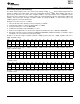
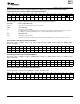
BIT # D15 D14 D13 D12 D11 D10 D9 D8 D7 D6 D5 D4 D3 D2 D1 D0
BIT
SIGN SD14_8 SD13_8 SD12_8 SD11_8 SD10_8 SD9_8 SD8_8 SD7_8 SD6_8 SD5_8 SD4_8 SD3_8 SD2_8 SD1_8 SD0_8
NAME
POR
0 0 0 0 0 0 0 0 0 0 0 0 0 0 0 0
VALUE
At PGA = ÷4, full-scale range = ±160mV (decimal = 16000, positive value hex = 3E80, negative value hex =
C180), and LSB = 10μV.
BIT # D15 D14 D13 D12 D11 D10 D9 D8 D7 D6 D5 D4 D3 D2 D1 D0
BIT
SIGN SIGN SD13_4 SD12_4 SD11_4 SD10_4 SD9_4 SD8_4 SD7_4 SD6_4 SD5_4 SD4_4 SD3_4 SD2_4 SD1_4 SD0_4
NAME
POR
0 0 0 0 0 0 0 0 0 0 0 0 0 0 0 0
VALUE
At PGA = ÷2, full-scale range = ±80mV (decimal = 8000, positive value hex = 1F40, negative value hex = E0C0),
and LSB = 10μV.
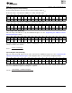
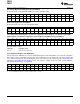
BIT # D15 D14 D13 D12 D11 D10 D9 D8 D7 D6 D5 D4 D3 D2 D1 D0
BIT
SIGN SIGN SIGN SD12_2 SD11_2 SD10_2 SD9_2 SD8_2 SD7_2 SD6_2 SD5_2 SD4_2 SD3_2 SD2_2 SD1_2 SD0_2
NAME
POR
0 0 0 0 0 0 0 0 0 0 0 0 0 0 0 0
VALUE
At PGA = ÷1, full-scale range = ±40mV (decimal = 4000, positive value hex = 0FA0, negative value hex = F060),
and LSB = 10μV.
BIT # D15 D14 D13 D12 D11 D10 D9 D8 D7 D6 D5 D4 D3 D2 D1 D0
BIT
SIGN SIGN SIGN SIGN SD11_1 SD10_1 SD9_1 SD8_1 SD7_1 SD6_1 SD5_1 SD4_1 SD3_1 SD2_1 SD1_1 SD0_1
NAME
POR
0 0 0 0 0 0 0 0 0 0 0 0 0 0 0 0
VALUE
Copyright © 2010–2011, Texas Instruments Incorporated 41