
Datasheet

1
2
3
4
5
6
7
V
IN-
SDA
SCL
A0
V
IN+
V+
Filter C
DXP2
DXN1
DXP1
GPIO
ALERT
GND
DXN2
14
13
12
11
10
9
8
TMP512
V
IN+
V
IN-
SDA
SCL
GPIO
DXN2
DXP2
DXN1
12
11
10
9
Filter C
1
2
3
4
5
6
7
8
13
14
15
16
A0
NC
NC
DXP1
ALERT
GND
V+
TMP512
TMP512
TMP513
SBOS491A –JUNE 2010– REVISED MAY 2011
www.ti.com
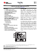
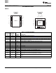
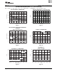
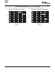
PIN CONFIGURATIONS
TMP512
space
D PACKAGE
RSA PACKAGE
SO-14
QFN-16
(TOP VIEW)
(TOP VIEW)
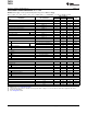
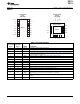
TMP512: PIN DESCRIPTIONS
RSA
D PACKAGE PACKAGE
SO-16 QFN-16 NAME DESCRIPTION
1 15 Filter C Subregulator output and filter capacitor pin.
2 16 V+ Positive supply voltage (3V to 26V) See Figure 22.
3 1 V
IN+
Positive differential shunt voltage. Connect to positive side of shunt resistor.
Negative differential shunt voltage. Connect to negative side of shunt resistor. Bus voltage is
4 2 V
IN-
measured from this pin to ground.
5 3 SDA Serial bus data line for SMBus, open-drain; requires pull-up resistor.
6 4 SCL Serial bus clock line for SMBus, open-drain; requires pull-up resistor.
7 5 A0 Address pin
— 6 NC Not connected
— 7 NC Not connected
8 8 DXP1 Channel 1 positive connection to remote temperature sensor.
9 9 DXN1 Channel 1 negative connection to remote temperature sensor.
10 10 DXP2 Channel 2 positive connection to remote temperature sensor.
11 11 DXN2 Channel 2 negative connection to remote temperature sensor.
General-purpose, user-programmable input/output. Totem-pole output. Connect to ground or
12 12 GPIO
supply through a resistor if not used. Default state is as an input.
Open-drain SMBus alert output. Controlled in SMBus Alert Mask Register. Default state is
13 13 ALERT
disabled.
14 14 GND Ground
6 Copyright © 2010–2011, Texas Instruments Incorporated