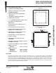
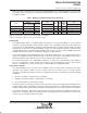
TMS320 SECOND-GENERATION DIGITAL SIGNAL PROCESSORS SPRS010B — MAY 1987 — REVISED NOVEMBER 1990 • • • • • • • • A 4K Words of On-Chip Program ROM (TMS320C25) C B D E 128K Words of Data/Program Space F 32-Bit ALU/Accumulator G 16 × 16-Bit Multiplier With a 32-Bit Product H J Block Moves for Data/Program Management K L Repeat Instructions for Efficient Use of Program Space 68-Pin FN and FZ Packages† (Top View) Serial Port for Direct Codec Interface Synchronization Input for Synchronous Multiproc
TMS320 SECOND-GENERATION DEVICES SPRS010B — MAY 1987 — REVISED NOVEMBER 1990 PGA AND PLCC/CER-QUAD PIN ASSIGNMENTS FUNCTION PIN FUNCTION PIN A0 K1/26 FUNCTION A12 K8/40 PIN D2 E1/16 FUNCTION D14 A5/3 PIN FUNCTION INT2 PIN A1 K2/28 A13 L9/41 D3 D2/15 D15 B6/2 A2 L3/29 A14 K9/42 D4 D1/14 DR J1/24 J11/46 MP/MC† A6/1 A3 K3/30 A15 L10/43 D5 C2/13 DS A4 L4/31 BIO B7/68 D6 C1/12 A5 K4/32 BR G11/50 D7 B2/11 A6 L5/33 CLKOUT1 C11/58 D8 A7 K5/34 CLKOUT2 D10/57
TMS320 SECOND-GENERATION DEVICES SPRS010B — MAY 1987 — REVISED NOVEMBER 1990 description The TMS320 family of 16/32-bit single-chip digital signal processors combines the flexibility of a high-speed controller with the numerical capability of an array processor, thereby offering an inexpensive alternative to multichip bit-slice processors.
TMS320 SECOND-GENERATION DEVICES SPRS010B — MAY 1987 — REVISED NOVEMBER 1990 Key Features: TMS32020 • • • • • • • • • • • +5 V GND 200-ns Instruction Cycle Time 544 Words of On-Chip Data RAM Interrupts 128K Words of Total Data/Program Memory Space Wait States for Communication to Slower Off-Chip Memories Source Code Compatible With the TMS320C1x 256-Word Data/Prog RAM 288-Word Data RAM Multiplier Data (16) MultiProcessor Interface 32-BIT ALU/ACC Serial Interface Single-Cycle Multiply/Accumulate
TMS320 SECOND-GENERATION DEVICES SPRS010B — MAY 1987 — REVISED NOVEMBER 1990 Table 1 provides an overview of the second-generation TMS320 processors with comparisons of memory, I/O, cycle timing, power, package type, technology, and military support. For specific availability, contact the nearest TI Field Sales Office. Table 1.
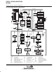
TMS320 SECOND-GENERATION DEVICES SPRS010B — MAY 1987 — REVISED NOVEMBER 1990 functional block diagram (TMS320C2x) SYNC IS DS PS X1 X2/CLKIN CLKOUT1 CLKOUT2 Program Bus R/W STRB READY BR XF HOLD HOLDA MSC BIO RS IACK 16 16 16 16 PFC(16) QIR(16) IR(16) 16 STO(16) Controller MUX ST1(16) 16 16 3 A15-A0 16 16 16 (8 x 16) RSR(16) XSR(16) 16 16 16 MUX D15-D0 DRR(16) 16 Instruction 16 DR CLKR FSR DX CLKX FSX 16 Stack Program ROM/ EPROM (4096 × 16) MUX 16 16 Address 16 MP/MC I
TMS320 SECOND-GENERATION DEVICES SPRS010B — MAY 1987 — REVISED NOVEMBER 1990 scaling shifter The TMS320C2x scaling shifter has 16-bit input connected to the data bus and a 32-bit output connected to the ALU. The scaling shifter produces a left shift of 0 to 16 bits on the input data, as programmed in the instruction.
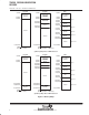
TMS320 SECOND-GENERATION DEVICES SPRS010B — MAY 1987 — REVISED NOVEMBER 1990 Program 0(0000h) Program 0(0000h) Interrupts and Reserved (External) 31(001Fh) 32(0020h ) 31(001Fh) 32(0020h ) 4015(0FAFh) 4016(0FB0h) Data 0(0000h) Interrupts and Reserved (On-Chip ROM/EPROM) On-Chip Memory-Mapped Registers 5(0005h) 6(0006h) Reserved On-Chip ROM/EPROM Page 0 95(005Fh) 96(0060h ) 127(007Fh) 128(0080h) Reserved 4095(0FFFh) 4096(1000h) On-Chip Block B2 Reserved Pages 1-3 On-Chip Block B0 Pages 4-5 On
TMS320 SECOND-GENERATION DEVICES SPRS010B — MAY 1987 — REVISED NOVEMBER 1990 interrupts and subroutines The TMS320C2x has three external maskable user interrupts INT2-INT0, available for external devices that interrupt the processor. Internal interrupts are generated by the serial port (RINT and XINT), by the timer (TINT), and by the software interrupt (TRAP) instruction.
TMS320 SECOND-GENERATION DEVICES SPRS010B — MAY 1987 — REVISED NOVEMBER 1990 instruction set The TMS320C2x microprocessor implements a comprehensive instruction set that supports both numeric-intensive signal processing operations as well as general-purpose applications, such as multiprocessing and high-speed control. The TMS32020 source code is upward-compatible with TMS320C25 source code. TMS32020 object code runs directly on the TMS320C25.
TMS320 SECOND-GENERATION DEVICES SPRS010B — MAY 1987 — REVISED NOVEMBER 1990 instruction set summary Table 2 lists the symbols and abbreviations used in Table 3, the TMS320C25 instruction set summary. Table 3 consists primarily of single-cycle, single-word instructions. Infrequently used branch, I/O, and CALL instructions are multicycle. The instruction set summary is arranged according to function and alphabetized within each functional grouping.
TMS320C25 SPRS010B — MAY 1987 — REVISED NOVEMBER 1990 Table 3. TMS320C25 Instruction Set Summary ACCUMULATOR MEMORY REFERENCE INSTRUCTIONS MNEMONIC INSTRUCTION BIT CODE NO.
TMS320C25 SPRS010B — MAY 1987 — REVISED NOVEMBER 1990 Table 3. TMS320C25 Instruction Set Summary (continued) ACCUMULATOR MEMORY REFERENCE INSTRUCTIONS MNEMONIC INSTRUCTION BIT CODE NO.
TMS320C25 SPRS010B — MAY 1987 — REVISED NOVEMBER 1990 Table 3. TMS320C25 Instruction Set Summary (continued) T REGISTER, P REGISTER, AND MULTIPLY INSTRUCTIONS MNEMONIC INSTRUCTION BIT CODE NO.
TMS320C25 SPRS010B — MAY 1987 — REVISED NOVEMBER 1990 Table 3. TMS320C25 Instruction Set Summary (continued) BRANCH/CALL INSTRUCTIONS MNEMONIC INSTRUCTION BIT CODE NO.
TMS320C25 SPRS010B — MAY 1987 — REVISED NOVEMBER 1990 Table 3. TMS320C25 Instruction Set Summary (concluded) CONTROL INSTRUCTIONS MNEMONIC INSTRUCTION BIT CODE NO.
TMS32020 SPRS010B — MAY 1987 — REVISED NOVEMBER 1990 TMS32020 PRODUCT NOTIFICATION Texas Instruments has identified an unusual set of circumstances that will cause the BIT (Test Bit) instruction on the TMS32020 to affect the contents of the accumulator; ideally, the BIT instruction should not affect the accumulator. This set of conditions is: 1. The overflow mode is set (the OVM status register bit is set to one.) 2. And, the two LSBs of the BIT instruction opcode word are zero. a.
TMS320 SECOND-GENERATION DEVICES SPRS010B — MAY 1987 — REVISED NOVEMBER 1990 development support Together, Texas Instruments and its authorized third-party suppliers offer an extensive line of development support products to assist the user in all aspects of TMS320 second-generation-based design and development. These products range from development and application software to complete hardware development and evaluation systems.
TMS320 SECOND-GENERATION DEVICES SPRS010B — MAY 1987 — REVISED NOVEMBER 1990 Table 4.
TMS320 SECOND-GENERATION DEVICES SPRS010B — MAY 1987 — REVISED NOVEMBER 1990 documentation support Extensive documentation supports the second-generation TMS320 devices from product announcement through applications development. The types of documentation include data sheets with design specifications, complete user’s guides, and 750 pages of application reports published in the book, Digital Signal Processing Applications with the TMS320 Family (SPRA012A).
TMS32020 SPRS010B — MAY 1987 — REVISED NOVEMBER 1990 absolute maximum ratings over specified temperature range (unless otherwise noted)† Supply voltage range, VCC‡ . . . . . . . . . . . . . . . . . . . . . . . . . . . . . . . . . . . . . . . . . . . . . . . . . . . . . . . . – 0.3 V to 7 V Input voltage range . . . . . . . . . . . . . . . . . . . . . . . . . . . . . . . . . . . . . . . . . . . . . . . . . . . . . . . . . . . . . . . – 0.3 V to 7 V Output voltage range . . . . . . . . . . . . . . . . . . .
TMS32020 SPRS010B — MAY 1987 — REVISED NOVEMBER 1990 CLOCK CHARACTERISTICS AND TIMING The TMS32020 can use either its internal oscillator or an external frequency source for a clock. internal clock option The internal oscillator is enabled by connecting a crystal across X1 and X2/CLKIN (see Figure 2). The frequency of CLKOUT1 is one-fourth the crystal fundamental frequency.
TMS32020 SPRS010B — MAY 1987 — REVISED NOVEMBER 1990 timing requirements over recommended operating conditions (see Note 3) MIN MAX UNIT 597 ns CLKIN fall time 10† ns tr(CI) CLKIN rise time 10† ns tw(CIL) CLKIN low pulse duration, tc(CI) = 50 ns (see Note 4) 40 ns tw(CIH) CLKIN high pulse duration, tc(CI) = 50 ns (see Note 4) 40 ns tsu(S) SYNC setup time before CLKIN low 10 th(S) SYNC hold time from CLKIN low 15 tc(C) tf(CI) CLKIN cycle time 195 NOM Q – 10 ns ns † Value deri
TMS32020 SPRS010B — MAY 1987 — REVISED NOVEMBER 1990 MEMORY AND PERIPHERAL INTERFACE TIMING switching characteristics over recommended operating conditions (see Note 3) PARAMETER TYP MAX Q – 15 MIN Q Q + 15 UNIT ns – 15 0 15 ns td(C1-S) STRB from CLKOUT1 (if STRB is present) td(C2-S) CLKOUT2 to STRB (if STRB is present) tsu(A) Address setup hold time before STRB low (see Note 5) Q – 30 ns th(A) Address hold time after STRB high (see Note 5) Q – 15 ns tw(SL) STRB low pulse duration
TMS32020 SPRS010B — MAY 1987 — REVISED NOVEMBER 1990 RS, INT, BIO, AND XF TIMING switching characteristics over recommended operating conditions (see Note 3 and 8) PARAMETER td(RS) CLKOUT1 low to reset state entered td(IACK) CLKOUT1 to IACK valid td(XF) XF valid before falling edge of STRB MIN TYP – 25 0 MAX UNIT 45 ns 25 ns Q – 30 ns NOTES: 3. Q = 1/4tc(C). 8. RS, INT, and BIO are asynchronous inputs and can occur at any time during a clock cycle.
TMS32020 SPRS010B — MAY 1987 — REVISED NOVEMBER 1990 SERIAL PORT TIMING switching characteristics over recommended operating conditions (see Note 3) PARAMETER MAX UNIT 100 ns DX valid after FSX falling edge (TXM = 0, see Note 10) 50 ns FSX valid after CLKX rising edge (TXM = 1) 60 ns td(CH-DX) DX valid after CLKX rising edge (see Note 10) td(FL-DX) td(CH-FS) MIN TYP NOTES: 3. Q = 1/4tc(C). 10. The last occurrence of FSX falling and CLKX rising.
TMS320C25, TMS320E25 SPRS010B — MAY 1987 — REVISED NOVEMBER 1990 absolute maximum ratings over specified temperature range (unless otherwise noted)† Supply voltage range, VCC‡ . . . . . . . . . . . . . . . . . . . . . . . . . . . . . . . . . . . . . . . . . . . . . . . . . . . . . . . . – 0.3 V to 7 V Input voltage range: TMS320E25 pins 24 and 25 . . . . . . . . . . . . . . . . . . . . . . . . . . . . . . . . . . . . . – 0.3 V to 15 V All other inputs . . . . . . . . . . . . . . . . . . . . . . . . . . . .
TMS320C25, TMS320E25 SPRS010B — MAY 1987 — REVISED NOVEMBER 1990 CLOCK CHARACTERISTICS AND TIMING The TMS32025 can use either its internal oscillator or an external frequency source for a clock. internal clock option The internal oscillator is enabled by connecting a crystal across X1 and X2/CLKIN (see Figure 2). The frequency of CLKOUT1 is one-fourth the crystal fundamental frequency.
TMS320C25, TMS320E25 SPRS010B — MAY 1987 — REVISED NOVEMBER 1990 timing requirements over recommended operating conditions (see Note 3) MIN MAX UNIT 150 ns CLKIN fall time 5† ns tr(CI) CLKIN rise time 5† ns tw(CIL) CLKIN low pulse duration, tc(CI) = 50 ns (see Note 4) 20 ns tw(CIH) CLKIN high pulse duration, tc(CI) = 50 ns (see Note 4) 20 ns tsu(S) SYNC setup time before CLKIN low 5 th(S) SYNC hold time from CLKIN low 8 tc(CI) tf(CI) CLKIN cycle time 24.
TMS320C25, TMS320E25 SPRS010B — MAY 1987 — REVISED NOVEMBER 1990 2.0 V 2.4 V VIH (Min) 1.88 V 0.92 V VIL (Max) 0.80 V VOH (Min) 2.2 V 0.8 V VOL (Max) 0.6 V 0 0 (a) Input (b) Output Figure 5.
TMS320C25, TMS320E25 SPRS010B — MAY 1987 — REVISED NOVEMBER 1990 RS, INT, BIO, AND XF TIMING switching characteristics over recommended operating conditions (see Note 3 and 8) PARAMETER td(RS) CLKOUT1 low to reset state entered td(IACK) CLKOUT1 to IACK valid td(XF) XF valid before falling edge of STRB MIN TYP –6 0 MAX 22† 12 Q – 15 UNIT ns ns ns NOTES: 3. Q = 1/4tc(C). 8. RS, INT, and BIO are asynchronous inputs and can occur at any time during a clock cycle.
TMS320C25, TMS320E25 SPRS010B — MAY 1987 — REVISED NOVEMBER 1990 SERIAL PORT TIMING switching characteristics over recommended operating conditions (see Note 3) PARAMETER MIN TYP MAX UNIT td(CH-DX) DX valid after CLKX rising edge (see Note 10) 75 ns td(FL-DX) DX valid after FSX falling edge (TXM = 0, see Note 10) 40 ns td(CH-FS) FSX valid after CLKX rising edge (TXM = 1) 40 ns NOTES: 3. Q = 1/4tc(C). 10. The last occurrence of FSX falling and CLKX rising.
TMS320E25 SPRS010B — MAY 1987 — REVISED NOVEMBER 1990 EPROM PROGRAMMING absolute maximum ratings over specified temperature range (unless otherwise noted)† Supply voltage range, VPP‡ . . . . . . . . . . . . . . . . . . . . . . . . . . . . . . . . . . . . . . . . . . . . . . . . . . . . . . . – 0.6 V to 15 V Input voltage range on pins 24 and 25 . . . . . . . . . . . . . . . . . . . . . . . . . . . . . . . . . . . . . . . . . . . . . . – 0.
TMS320C25-50 SPRS010B — MAY 1987 — REVISED NOVEMBER 1990 absolute maximum ratings over specified temperature range (unless otherwise noted)† Supply voltage range, VCC‡ . . . . . . . . . . . . . . . . . . . . . . . . . . . . . . . . . . . . . . . . . . . . . . . . . . . . . . . . – 0.3 V to 7 V Input voltage range . . . . . . . . . . . . . . . . . . . . . . . . . . . . . . . . . . . . . . . . . . . . . . . . . . . . . . . . . . . . . . . – 0.3 V to 7 V Output voltage range . . . . . . . . . . . . . . . . .
TMS320C25-50 SPRS010B — MAY 1987 — REVISED NOVEMBER 1990 CLOCK CHARACTERISTICS AND TIMING The TMS320C25-50 can use either its internal oscillator or an external frequency source for a clock. internal clock option The internal oscillator is enabled by connecting a crystal across X1 and X2, CLKIN. The frequency of CLKOUT1 is one-fourth the crystal fundamental frequency.
TMS320C25-50 SPRS010B — MAY 1987 — REVISED NOVEMBER 1990 +5 V TMS320C25 fcrystal 10 kΩ 74HC04 4.7 kΩ F11 CLKIN C = 20 pF 47 pF 0.1 µF 74AS04 10 kΩ L fcrystal, (MHz) ADVANCE INFORMATION TMS320C25 TMS320C25-50 TMS320E25 40.96 51.20 40.96 L, (µH) 1.8 1.0 1.8 Figure 7. External Clock Option timing requirements over recommended operating conditions (see Note 3) MIN 19.
TMS320C25-50 SPRS010B — MAY 1987 — REVISED NOVEMBER 1990 MEMORY AND PERIPHERAL INTERFACE TIMING switching characteristics over recommended operating conditions (see Note 3) MIN td(C1-S) STRB from CLKOUT (if STRB is present) td(C2-S) CLKOUT2 to STRB (if STRB is present) tsu(A) Address setup time before STRB low (see Note 5) tn(A) Address hold time after STRB high (see Note 5) tw(SL) STRB low pulse duration (no wait states, see Note 6) TYP MAX UNIT Q–5 Q+3 ns –2 5 ns Q – 11 ns Q–4 ns
TMS320C25-50 SPRS010B — MAY 1987 — REVISED NOVEMBER 1990 RS, INT, BIO, AND XF TIMING switching characteristics over recommended operating conditions (see Notes 3 and 16) PARAMETER td(RS) CLKOUT1 low to reset state entered td(IACK) CLKOUT1 to IACK valid td(XF) XF valid before falling edge of STRB MIN TYP –5 MAX 22† 7 Q–8 UNIT ns ns ns † Value derived from characterization data and not tested. NOTES: 3. Q = 1/4 tc(C) 16.
TMS320C25-50 SPRS010B — MAY 1987 — REVISED NOVEMBER 1990 SERIAL PORT TIMING switching characteristics over recommended operating conditions (see Note 3) PARAMETER MIN TYP MAX UNIT td(CH-DX) DX valid after CLKX rising edge (see Note 18) 75 ns td(FL-DX) DX valid after falling edge (TXM = 0, see Note 18) 40 ns td(CH-FS) FSX valid after CLKX raising edge (TXM = 1) 40 ns NOTES: 3. Q = 1/4 tc(C) 18. The last occurrence of FSX falling and CLKX rising.
TMS320C25-50 SPRS010B — MAY 1987 — REVISED NOVEMBER 1990 memory and peripheral interface timing TMS320C25 PARAMETER td(C1-S) td(C2-S) tsu(A) th(A) TMS320C25-50 TYP MAX MIN Q –6 Q Q+6 Q–5 Q+3 ns –6 0 6 –2 5 ns Q – 12 TYP Q – 11 Q–8 ns Q–4 tw(SL) tw(SH) ns 2Q 2Q – 5 2Q + 2 ns 2Q 2Q – 2 2Q + 5 ns tsu(D)W th(D)W 2Q – 20 Q – 10 Q td(MSC) ta(A) – 12 0 2Q – 17 ns Q–5 ns tsu(D)R th(D)R 23 19 0 0 12 –1 3Q – 35 ADVANCE INFORMATION td(SL-R) td(C2H-R) ns ns ns Q –
TMS320 SECOND-GENERATION DEVICES SPRS010B — MAY 1987 — REVISED NOVEMBER 1990 TIMING DIAGRAMS This section contains all the timing diagrams for the TMS320 second-generation devices. Refer to the top corner of page for the specific device. Timing measurements are referenced to and from a low voltage of 0.8 voltage and a high voltage of 2 volts, unless otherwise noted.
TMS320 SECOND-GENERATION DEVICES SPRS010B — MAY 1987 — REVISED NOVEMBER 1990 memory read timing td(C1-S) CLKOUT1 td(C1-S) CLKOUT2 td(C2-S) td(C2-S) STRB tw(SH) tsu(A) th(A) tw(SL) ADVANCE INFORMATION A15-A0, BR, PS, DS or IS Valid ta(A) R/W td(SL-R) tsu(D)R READY th(SL-R) th(D)R D15-D0 42 Data In POST OFFICE BOX 1443 • HOUSTON, TEXAS 77001
TMS320 SECOND-GENERATION DEVICES SPRS010B — MAY 1987 — REVISED NOVEMBER 1990 memory write timing CLKOUT1 CLKOUT2 STRB th(A) tsu(A) A15-A0, BR, PS, DS or IS ADVANCE INFORMATION Valid R/W READY tsu(D)W D15-D0 th(D)W Data Out ten(D) POST OFFICE BOX 1443 • HOUSTON, TEXAS 77001 tdis(D) 43
TMS320 SECOND-GENERATION DEVICES SPRS010B — MAY 1987 — REVISED NOVEMBER 1990 one wait-state memory access timing CLKOUT1 CLKOUT2 STRB th(C2H-R) A15-A0, BR, PS, DS, R/W or IS Valid ADVANCE INFORMATION td(C2H-R) th(C2H-R) td(C2H-R) READY td(M-R) D15-D0 (For Read Operation) th(M-R) th(M-R) td(M-R) Data In D15-D0 (For Write Operation) Data Out td(MSC) td(MSC) MSC 44 POST OFFICE BOX 1443 • HOUSTON, TEXAS 77001
TMS320 SECOND-GENERATION DEVICES SPRS010B — MAY 1987 — REVISED NOVEMBER 1990 reset timing CLKOUT1 tsu(IN) td(RS) tsu(IN) th(IN) RS tw(RS) A15-A0 Valid Fetch Location 0 D15-D0 PS Begin Program Execution ADVANCE INFORMATION Valid STRB Control Signals† IACK Serial Port Control‡ † Control signals are DS, IS, R/W, and XF. ‡ Serial port controls are DX and FSX.
TMS320 SECOND-GENERATION DEVICES SPRS010B — MAY 1987 — REVISED NOVEMBER 1990 interrupt timing (TMS32020) CLKOUT1 STRB tsu(IN) th(IN) tw(IN) INT2-INT0 td(IACK) tf(IN) A15-A0 FETCH N FETCH N + 1 FETCH I FETCH I + 1 ADVANCE INFORMATION td(IACK) IACK interrupt timing (TMS320C25) CLKOUT1 tsu(IN) STRB th(IN) tw(IN) INT2-INT0 tf(IN) A15-A0 FETCH N td(IACK) FETCH N + 1 FETCH N + 2 td(IACK) IACK 46 POST OFFICE BOX 1443 • HOUSTON, TEXAS 77001 N+3 FETCH I
TMS320 SECOND-GENERATION DEVICES SPRS010B — MAY 1987 — REVISED NOVEMBER 1990 serial port receive timing tc(SCK) tr(SCK) tw(SCK) CLKR th(DR) tf(SCK) th(FS) tw(SCK) FSR tsu(FS) ADVANCE INFORMATION tsu(DR) DR serial port transmit timing tc(SCK) tr(SCK) tw(SCK) CLKX td(CH-DX) tf(SCK) tw(SCK) th(FS) FSX (Input, TXM = 0) tsu(FS) td(CH-DX) td(FL-DX) DX N=1 td(CH-FS) N = 8,16 td(CH-FS) FSX (Output, TXM = 1) POST OFFICE BOX 1443 • HOUSTON, TEXAS 77001 47
TMS32020 SPRS010B — MAY 1987 — REVISED NOVEMBER 1990 BIO timing CLKOUT1 STRB FETCH Branch Address FETCH Next Instruction FETCH BIOZ A15-A0 PC = N PC = N + 1 PC = N + 2 PC = N + 3 or Branch Address tsu(IN) th(IN) ADVANCE INFORMATION BIO Valid external flag timing CLKOUT1 STRB td(XF) A15-A0 Valid FETCH SXF/RXF Valid Valid PC = N – 1 PC = N PC = N + 1 PC = N + 2 XF 48 Valid POST OFFICE BOX 1443 • HOUSTON, TEXAS 77001
TMS320C25 SPRS010B — MAY 1987 — REVISED NOVEMBER 1990 BIO timing CLKOUT1 STRB FETCH Branch Address FETCH Next Instruction FETCH BIOZ A15-A0 PC = N PC = N + 1 PC = N + 2 or Branch Address tsu(IN) BIO ADVANCE INFORMATION th(IN) Valid external flag timing CLKOUT1 STRB td(XF) A15-A0 FETCH SXF/RXF Valid Valid Valid PC = N PC = N + 1 PC = N + 2 PC = N + 3 XF Valid POST OFFICE BOX 1443 • HOUSTON, TEXAS 77001 49
TMS32020 SPRS010B — MAY 1987 — REVISED NOVEMBER 1990 HOLD timing (part A) CLKOUT1 CLKOUT2 STRB td(C2H-H)† HOLD ADVANCE INFORMATION A15-A0 N N+1 PS, DS, or IS Valid Valid N+2 R/W tdis(C1L-A) D15-D0 In In tdis(AL-A) HOLDA td(C1L-AL) FETCH EXECUTE N N+1 N/A N/A N–1 N Dummy Dead † HOLD is an asynchronous input and can occur at any time during a clock cycle. If the specified timing is met, the exact sequence shown will occur; otherwise, a delay of one CLKOUT2 cycle will occur.
TMS32020 SPRS010B — MAY 1987 — REVISED NOVEMBER 1990 HOLD timing (part B) CLKOUT1 CLKOUT2 ten(A-C1L) STRB td(C2H-H)† Valid A15-A0 ADVANCE INFORMATION HOLD Valid PS, DS, or IS R/W In In N+2 N+3 td(HH-AH) D15-D0 HOLDA FETCH EXECUTE N/A N /A N+2 N+3 Dead Dead N+1 N+2 † HOLD is an asynchronous input and can occur at any time during a clock cycle. If the specified timing is met, the exact sequence shown will occur; otherwise, a delay of one CLKOUT2 cycle will occur.
TMS320C25 SPRS010B — MAY 1987 — REVISED NOVEMBER 1990 HOLD timing (part A) CLKOUT1 CLKOUT2 STRB td(C2H-H)† HOLD ADVANCE INFORMATION A15-A0 N N+1 PS, DS, or IS Valid Valid N+2 R/W tdis(C1L-A) D15-D0 In In tdis(AL-A) HOLDA td(C1L-AL) FETCH EXECUTE N N+1 – – N–2 N –1 N – † HOLD is an asynchronous input and can occur at any time during a clock cycle. If the specified timing is met, the exact sequence shown will occur; otherwise, a delay of one CLKOUT2 cycle will occur.
TMS320C25 SPRS010B — MAY 1987 — REVISED NOVEMBER 1990 HOLD timing (part B) CLKOUT1 CLKOUT2 ten(A-C1L) STRB td(C2H-H)† ADVANCE INFORMATION HOLD Valid PS, DS, or IS R/W D15-D0 In td(HH-AH) HOLDA A15-A0 FETCH EXECUTE N+2 N+2 – – – N+2 – – – N+1 † HOLD is an asynchronous input and can occur at any time during a clock cycle. If the specified timing is met, the exact sequence shown will occur; otherwise, a delay of one CLKOUT2 cycle will occur.
TMS320 SECOND-GENERATION DEVICES SPRS010B — MAY 1987 — REVISED NOVEMBER 1990 TYPICAL SUPPLY CURRENT CHARACTERISTICS FOR TMS320C25 ICC vs f(CLKIN) and VCC Powerdown Mode 170 160 150 140 130 120 110 100 90 80 70 60 50 40 30 20 10 80 TA = 25°C VCC = 5.50 V VCC = 5.25 V VCC = 5.00 V VCC = 4.75 V VCC = 4.50 V VCC = 5.50 V VCC = 5.25 V VCC = 5.00 V VCC = 4.75 V VCC = 4.
TMS320 SECOND-GENERATION DEVICES SPRS010B — MAY 1987 — REVISED NOVEMBER 1990 MECHANICAL DATA 68-pin GB grid array ceramic package (TMS32020, TMS320C25) 28,448 (1.120) 27,432 (1.080) Thermal Resistance Characteristics MAX UNIT RθJA Junction-to-free-air thermal resistance 36 °C/W RθJC Junction-to-case thermal resistance 6 °C/W 28,448 (1.120) 27,432 (1.080) 17,02 (0.670) Nom 4,953 (0.195) 2,032 (0.080) 3,302 (0.130) 2,794 (0.110) ADVANCE INFORMATION PARAMETER 17,02 (0.670) Nom 1,397 (0.
TMS320C25 TMS320C25-50 SPRS010B — MAY 1987 — REVISED NOVEMBER 1990 68-lead plastic leaded chip carrier package (TMS320C25 and TMS320C25-50) Seating Plane 0,25 (0.010) R Max 3 Places 24,33 (0.956) 24,13 (0.950) (see Note A) 1,27 (0.050) T.P. (see Note B) 23,62 (0.930) 23,11 (0.910) (At Seating Plane) 25,27 (0.995) 25,02 (0.985) ADVANCE INFORMATION 0,94 (0.037) 0,69 (0.027) R 1,22 (0.048) × 45° 1,07 (0.042) 1,35 (0.053) × 45° 1,19 (0.047) 24,33 (0.956) 24,13 (0.950) (see Note A) 2,79 (0.
TMS320E25 SPRS010B — MAY 1987 — REVISED NOVEMBER 1990 MECHANICAL DATA 68-lead FZ CER-QUAD, ceramic leaded chip carrier package (TMS320E25 only) This hermetically-sealed chip carrier package consists of a ceramic base, ceramic cap, and a 68-lead frame. Hermetic sealing is accomplished with glass. The FZ package is intended for both socket- or surface- mounting. Having a Sn/Pb ratio of 60/40, the tin/lead-coated leads do not require special cleaning or processing when being surface-mounted. 4,57 (0.
TMS320E25 SPRS010B — MAY 1987 — REVISED NOVEMBER 1990 programming the TMS320E25 EPROM cell The TMS320E25 includes a 4K × 16-bit EPROM, implemented from an industry-standard EPROM cell, to perform prototyping and early field testing and to achieve low-volume production. When used with a 4K-word masked-ROM TMS320C25, the TMS320E25 yields a high-volume, low-cost production as a result of more migration paths for data.
TMS320E25 SPRS010B — MAY 1987 — REVISED NOVEMBER 1990 RS Figure 9 shows the wiring conversion to program the TMS320E25 using the 28-pin pinout of the TMS27C64. The pin nomenclature table provides a description of the TMS27C64 pins. The code to be programmed into the device should be serial mode. The TMS320E25 uses 13 address lines to address the 4K-word memory in byte format.
TMS320E25 SPRS010B — MAY 1987 — REVISED NOVEMBER 1990 Table 5 shows the programming levels required for programming, verifying and reading the EPROM cell. The paragraphs following the table describe the function of each programming level. Table 5.
TMS320E25 SPRS010B — MAY 1987 — REVISED NOVEMBER 1990 program verify Programmed bits may be verified with VPP = 12.5 V when G = VIL, E = VIL, and PGM = VIH. Figure 11 shows the timing for the program and verify operation. Start Address = First Location VCC = 6 ± 0.25 V VPP = 12.5 V ± 0.
TMS320E25 SPRS010B — MAY 1987 — REVISED NOVEMBER 1990 Program Verify VIH A12-A0 Address Stable Address N + 1 VIL VIH/VOH Q8-Q1 Data In Stable HI-Z Data Out Valid VIL/VOL VPP VPP VCC VCC + 1 VCC VCC ADVANCE INFORMATION VIH E VIL VIH PGM VIL VIH G VIL Figure 11. Fast Programming Timing program inhibit Programming may be inhibited by maintaining a high level input on the E pin or PGM pin.
TMS320E25 SPRS010B — MAY 1987 — REVISED NOVEMBER 1990 SIGNAL † TMS320E25 PIN TMS27C64 PIN ROM PROTECT PROTECT VERIFY VIH VIH VIL VIL VIH VPP VIH VCC VCC + 1 VSS VCC VSS VSS VSS VSS VSS E 22 20 G 42 22 PGM 41 27 VPP VCC VSS 25 1 61,35 28 10, 27, 44 14 CLKIN 52 14 RS 65 14 EPT 24 26 Q8-Q1 18-11 11-13, 15-19 VPP Q8 = PULSE VPP Q8 = RBIT A12-A10 40-38 2, 23, 21, X X A9-A7 37, 36, 34 24, 25, 3 X X A6 33 4 X A5 32 5 X VIL X A4 31 6 A3-A0 30-28, 26
TMS320E25 SPRS010B — MAY 1987 — REVISED NOVEMBER 1990 Start Program One Pulse of 3X-ms Duration X=0 EPROM Protect Setup Protect Verify Setup Program One 1-ms Pulse Device Failed Verify RBIT Device Passed X=X+1 Yes ADVANCE INFORMATION X = 25? No Protect Verify Setup Fail Verify RBIT Pass EPROM Protect Setup Figure 12. EPROM Protect Flowchart protect verify Protect verify is used following the EPROM protect to verify correct programming of the RBIT (see Figure 12).
TMS320E25 SPRS010B — MAY 1987 — REVISED NOVEMBER 1990 Protect Verify VIH A4 VIL VPP VPP VCC VCC + 1 VCC VCC VIL VIH PGM VIL VIH G VIL VIH/VOH Q8 HI-Z HI-Z HI-Z VIL/VOL VPP EPT VSS VIH A6 VIL Figure 13.
TMS320 SECOND-GENERATION DEVICES INDEX SPRS010B — MAY 1987 — REVISED NOVEMBER 1990 ADVANCE INFORMATION 66 POST OFFICE BOX 1443 • HOUSTON, TEXAS 77001
NIL NIL NIL SPRS010B — MAY 1987 — REVISED NOVEMBER 1990 accumulator . . . . . . . . . . . . . . . . . . . . . . . . . . . . . . . adapter socket . . . . . . . . . . . . . . . . . . . . . . . . . . . . addressing modes . . . . . . . . . . . . . . . . . . . . . . . . . ALU . . . . . . . . . . . . . . . . . . . . . . . . . . . . . . . . . . . . . . . architecture . . . . . . . . . . . . . . . . . . . . . . . . . . . . . . . . microcomputer/microprocessor mode multiplier . . . . . . . . . . . . . . . . . . .
PACKAGE OPTION ADDENDUM www.ti.
IMPORTANT NOTICE Texas Instruments Incorporated and its subsidiaries (TI) reserve the right to make corrections, modifications, enhancements, improvements, and other changes to its products and services at any time and to discontinue any product or service without notice. Customers should obtain the latest relevant information before placing orders and should verify that such information is current and complete.