
Car Stereo System User Manual

TMS320E25
SPRS010B — MAY 1987 — REVISED NOVEMBER 1990
POST OFFICE BOX 1443 • HOUSTON, TEXAS 77001
33
EPROM PROGRAMMING
absolute maximum ratings over specified temperature range (unless otherwise noted)
†
Supply voltage range, V
PP
‡
– 0.6 V to 15 V. . . . . . . . . . . . . . . . . . . . . . . . . . . . . . . . . . . . . . . . . . . . . . . . . . . . . . .
Input voltage range on pins 24 and 25 – 0.3 V to 15 V. . . . . . . . . . . . . . . . . . . . . . . . . . . . . . . . . . . . . . . . . . . . . .
†
Stresses beyond those listed under “Absolute Maximum Ratings” may cause permanent damage to the device. This is a stress rating only, and
functional operation of the device at these or any other conditions beyond those indicated in the “Recommended Operating Conditions” section of
this specification is not implied. Exposure to absolute-maximum-rated conditions for extended periods may affect device reliability.
‡
All voltage values are with respect to GND.
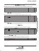
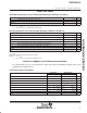
recommended operating conditions
MIN NOM MAX UNIT
V
CC
Programming mode supply voltage (see Note 13) 6 V
V
CC
Read mode supply voltage 4.75 5 5.25 V
V
PP
Programming mode supply voltage 12 12.5 13 V
V
PP
Read mode supply voltage (see Note 12) V
CC
V
NOTES: 12. V
PP
can be connected to V
CC
directly (except in the program mode). V
CC
supply current in this case would be I
CC
+ I
PP
. During
programming, V
PP
must be maintained at 12.5 V (± 0.25 V).
13. V
CC
must be applied before or at the same time as V
PP
and removed after or at the same time as V
PP
. This device must not be
inserted into or removed from the board when V
PP
or V
CC
is applied.
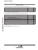
electrical characteristics over specified temperature range (unless otherwise noted)
PARAMETER TEST CONDITIONS MIN TYP
§
MAX UNIT
I
PP1
V
PP
supply current V
PP
= V
CC
= 5.25 V 100 µA
I
PP2
V
PP
supply current (during program pulse) V
PP
= 13 V 30 50 mA
§
All typical values for I
CC
are at V
CC
= 5 V, T
A
= 25°C.
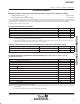
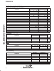
recommended timing requirements for programming, T
A
= 25°C, V
CC
= 6 V, V
PP
= 12.5 V
(see Notes 14 and 15)
MIN NOM MAX UNIT
t
w(IPGM)
Initial program pulse duration 0.95 1 1.05 ms
t
w(FPGM)
Final pulse duration 2.85 78.75 ms
t
su(A)
Address setup time 2 µs
t
su(E)
E setup time 2 µs
t
su(G)
G setup time 2 µs
t
dis(G)
Output disable time from G 0 130¶ ns
t
en(G)
Output enable time from G 150¶ ns
t
su(D)
Data setup time 2 µs
t
su(VPP)
V
PP
setup time 2 µs
t
su(VCC)
V
CC
setup time 2 µs
t
h(A)
Address hold time 0 µs
t
h(D)
Data hold time 2 µs
¶
Value derived from characterization data and not tested.
NOTES: 14. For all switching characteristics and timing measurements, input pulse levels are 0.4 V to 2.4 V and V
PP
= 12.5 V ± 0.5 V during
programming.
15. Common test conditions apply for t
dis(G)
except during programming.
ADVANCE INFORMATION