
Calculator User Manual
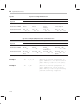
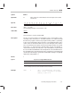
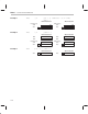
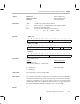
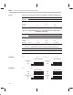
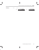
Table Of Contents
- Read This First
- Contents
- Figures
- Tables
- Examples
- Cautions
- Introduction
- Architectural Overview
- Central Processing Unit
- Memory and I/O Spaces
- Program Control
- Addressing Modes
- Assembly Language Instructions
- Instruction Set Summary
- How To Use the Instruction Descriptions
- Instruction Descriptions
- ABS
- ABS
- ADD
- ADD
- ADD
- ADD
- ADDC
- ADDC
- ADDS
- ADDS
- ADDT
- ADDT
- ADRK
- AND
- AND
- AND
- APAC
- APAC
- B
- BACC
- BANZ
- BANZ
- BCND
- BCND
- BIT
- BIT
- BITT
- BITT
- BLDD
- BLDD
- BLDD
- BLDD
- BLDD
- BLPD
- BLPD
- BLPD
- BLPD
- CALA
- CALL
- CC
- CC
- CLRC
- CLRC
- CMPL
- CMPR
- DMOV
- DMOV
- IDLE
- IN
- IN
- INTR
- LACC
- LACC
- LACC
- LACL
- LACL
- LACL
- LACT
- LACT
- LAR
- LAR
- LAR
- LDP
- LDP
- LPH
- LPH
- LST
- LST
- LST
- LST
- LT
- LT
- LTA
- LTA
- LTD
- LTD
- LTD
- LTP
- LTP
- LTS
- LTS
- MAC
- MAC
- MAC
- MAC
- MACD
- MACD
- MACD
- MACD
- MACD
- MAR
- MAR
- MPY
- MPY
- MPY
- MPYA
- MPYA
- MPYS
- MPYS
- MPYU
- MPYU
- NEG
- NEG
- NMI
- NOP
- NORM
- NORM
- NORM
- OR
- OR
- OR
- OUT
- OUT
- PAC
- POP
- POP
- POPD
- POPD
- PSHD
- PSHD
- PUSH
- RET
- RETC
- ROL
- ROR
- RPT
- RPT
- SACH
- SACH
- SACL
- SACL
- SAR
- SAR
- SBRK
- SETC
- SETC
- SFL
- SFR
- SFR
- SPAC
- SPH
- SPH
- SPL
- SPL
- SPLK
- SPLK
- SPM
- SQRA
- SQRA
- SQRS
- SQRS
- SST
- SST
- SUB
- SUB
- SUB
- SUB
- SUBB
- SUBB
- SUBC
- SUBC
- SUBS
- SUBS
- SUBT
- SUBT
- TBLR
- TBLR
- TBLR
- TBLW
- TBLW
- TBLW
- TRAP
- XOR
- XOR
- XOR
- ZALR
- ZALR
- On-Chip Peripherals
- Synchronous Serial Port
- Asynchronous Serial Port
- TMS320C209
- Register Summary
- TMS320C1x/C2x/C2xx/C5x Instruction Set Comparison
- Program Examples
- Submitting ROM Codes to TI
- Design Considerations for Using XDS510 Emulator
- E.1 Designing Your Target System’s Emulator Connector (14-Pin Header)
- E.2 Bus Protocol
- E.3 Emulator Cable Pod
- E.4 Emulator Cable Pod Signal Timing
- E.5 Emulation Timing Calculations
- E.6 Connections Between the Emulator and the Target System
- E.7 Physical Dimensions for the 14-Pin Emulator Connector
- E.8 Emulation Design Considerations
- Glossary
- Index

Load Accumulator With Shift
LACC
7-73
Assembly Language Instructions
Execution Increment PC, then ...
Event Addressing mode
(data-memory address) × 2
shift
→ ACC Direct or indirect
(data-memory address) × 2
16
→ ACC Direct or indirect (shift of 16)
lk × 2
shift
→ ACC Long immediate
Status Bits
Affected by
SXM
Description The contents of the specified data-memory address or a 16-bit constant are
left shifted and loaded into the accumulator. During shifting, low-order bits are
zero filled. High-order bits are sign extended if SXM = 1 and zeroed if SXM = 0.
Words
Words Addressing mode
1 Direct or indirect
2 Long immediate
Cycles for a Single LACC Instruction (Using Direct and Indirect Addressing)
Program
Operand ROM DARAM SARAM External
DARAM 1 1 1 1+p
SARAM 1 1 1, 2
†
1+p
External 1+d 1+d 1+d 2+d+p
†
If the operand and the code are in the same SARAM block
Cycles for a Repeat (RPT) Execution of an LACC Instruction (Using Direct
and Indirect Addressing)
Program
Operand ROM DARAM SARAM External
DARAM n n n n+p
SARAM n n n, n+1
†
n+p
External n+nd n+nd n+nd n+1+p+nd
†
If the operand and the code are in the same SARAM block
Cycles for a Single LACC Instruction (Using Immediate Addressing)
ROM DARAM SARAM External
2 2 2 2+2p
Cycles