
Calculator User Manual
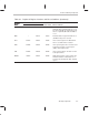
Table Of Contents
- Read This First
- Contents
- Figures
- Tables
- Examples
- Cautions
- Introduction
- Architectural Overview
- Central Processing Unit
- Memory and I/O Spaces
- Program Control
- Addressing Modes
- Assembly Language Instructions
- Instruction Set Summary
- How To Use the Instruction Descriptions
- Instruction Descriptions
- ABS
- ABS
- ADD
- ADD
- ADD
- ADD
- ADDC
- ADDC
- ADDS
- ADDS
- ADDT
- ADDT
- ADRK
- AND
- AND
- AND
- APAC
- APAC
- B
- BACC
- BANZ
- BANZ
- BCND
- BCND
- BIT
- BIT
- BITT
- BITT
- BLDD
- BLDD
- BLDD
- BLDD
- BLDD
- BLPD
- BLPD
- BLPD
- BLPD
- CALA
- CALL
- CC
- CC
- CLRC
- CLRC
- CMPL
- CMPR
- DMOV
- DMOV
- IDLE
- IN
- IN
- INTR
- LACC
- LACC
- LACC
- LACL
- LACL
- LACL
- LACT
- LACT
- LAR
- LAR
- LAR
- LDP
- LDP
- LPH
- LPH
- LST
- LST
- LST
- LST
- LT
- LT
- LTA
- LTA
- LTD
- LTD
- LTD
- LTP
- LTP
- LTS
- LTS
- MAC
- MAC
- MAC
- MAC
- MACD
- MACD
- MACD
- MACD
- MACD
- MAR
- MAR
- MPY
- MPY
- MPY
- MPYA
- MPYA
- MPYS
- MPYS
- MPYU
- MPYU
- NEG
- NEG
- NMI
- NOP
- NORM
- NORM
- NORM
- OR
- OR
- OR
- OUT
- OUT
- PAC
- POP
- POP
- POPD
- POPD
- PSHD
- PSHD
- PUSH
- RET
- RETC
- ROL
- ROR
- RPT
- RPT
- SACH
- SACH
- SACL
- SACL
- SAR
- SAR
- SBRK
- SETC
- SETC
- SFL
- SFR
- SFR
- SPAC
- SPH
- SPH
- SPL
- SPL
- SPLK
- SPLK
- SPM
- SQRA
- SQRA
- SQRS
- SQRS
- SST
- SST
- SUB
- SUB
- SUB
- SUB
- SUBB
- SUBB
- SUBC
- SUBC
- SUBS
- SUBS
- SUBT
- SUBT
- TBLR
- TBLR
- TBLR
- TBLW
- TBLW
- TBLW
- TRAP
- XOR
- XOR
- XOR
- ZALR
- ZALR
- On-Chip Peripherals
- Synchronous Serial Port
- Asynchronous Serial Port
- TMS320C209
- Register Summary
- TMS320C1x/C2x/C2xx/C5x Instruction Set Comparison
- Program Examples
- Submitting ROM Codes to TI
- Design Considerations for Using XDS510 Emulator
- E.1 Designing Your Target System’s Emulator Connector (14-Pin Header)
- E.2 Bus Protocol
- E.3 Emulator Cable Pod
- E.4 Emulator Cable Pod Signal Timing
- E.5 Emulation Timing Calculations
- E.6 Connections Between the Emulator and the Target System
- E.7 Physical Dimensions for the 14-Pin Emulator Connector
- E.8 Emulation Design Considerations
- Glossary
- Index

Control of On-Chip Peripherals
8-2
8.1 Control of On-Chip Peripherals
The on-chip peripherals are controlled by accessing control registers that are
mapped to on-chip I/O space. Data is also transferred to and from the peripher-
als through these registers. Setting and clearing bits in these registers can en-
able, disable, initialize, and dynamically reconfigure the on-chip peripherals.
On a device reset, the CPU sends an internal SRESET signal to the peripheral
circuits. Table 8–1 lists the peripheral registers and summarizes what hap-
pens when the values in these registers are reset. For a description of all the
effects of a device reset, see Section 5.7,
Reset Operation
, on page 5-33.
Table 8–1. Peripheral Register Locations and Reset Conditions
Register
I/O Address
Register
Name
’C209
Other ’C2xx Reset Value Effects at Reset
CLK
– FFE8h 0000h
CLKOUT1-pin control (CLK) register.
The
CLKOUT1 signal is available at the
CLKOUT1 pin.
SDTR – FFF0h xxxxh
Synchronous data transmit and receive
register.
The value in this register is unde-
fined after reset.
SSPCR – FFF1h 0030h
Synchronous serial port control register.
The port emulation mode is set to immedi-
ate stop. Error and status flags are reset.
Receive interrupts are set to occur when the
receive buffer is not empty. Transmit inter-
rupts are set to occur when the transmit
buffer can accept one or more words. Exter-
nal clock and frame synchronization
sources are selected. Continuous mode is
selected. Digital loopback mode is disabled.
The receiver and transmitter are enabled.
ADTR – FFF4h xxxxh
Asynchronous data transmit and receive
register.
The value in this register is unde-
fined after reset.
ASPCR
– FFF5h 0000h
Asynchronous serial port control register.
The port emulation mode is set to immedi-
ate stop. Receive, transmit, and delta in-
terrupts are disabled. One stop bit is se-
lected. Auto-baud alignment is disabled.
The TX pin is forced high between trans-
missions. I/O pins IO0, IO1, IO2, and IO3
are configured as inputs. The port is
disabled.