
Calculator User Manual
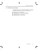
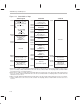
Table Of Contents
- Read This First
- Contents
- Figures
- Tables
- Examples
- Cautions
- Introduction
- Architectural Overview
- Central Processing Unit
- Memory and I/O Spaces
- Program Control
- Addressing Modes
- Assembly Language Instructions
- Instruction Set Summary
- How To Use the Instruction Descriptions
- Instruction Descriptions
- ABS
- ABS
- ADD
- ADD
- ADD
- ADD
- ADDC
- ADDC
- ADDS
- ADDS
- ADDT
- ADDT
- ADRK
- AND
- AND
- AND
- APAC
- APAC
- B
- BACC
- BANZ
- BANZ
- BCND
- BCND
- BIT
- BIT
- BITT
- BITT
- BLDD
- BLDD
- BLDD
- BLDD
- BLDD
- BLPD
- BLPD
- BLPD
- BLPD
- CALA
- CALL
- CC
- CC
- CLRC
- CLRC
- CMPL
- CMPR
- DMOV
- DMOV
- IDLE
- IN
- IN
- INTR
- LACC
- LACC
- LACC
- LACL
- LACL
- LACL
- LACT
- LACT
- LAR
- LAR
- LAR
- LDP
- LDP
- LPH
- LPH
- LST
- LST
- LST
- LST
- LT
- LT
- LTA
- LTA
- LTD
- LTD
- LTD
- LTP
- LTP
- LTS
- LTS
- MAC
- MAC
- MAC
- MAC
- MACD
- MACD
- MACD
- MACD
- MACD
- MAR
- MAR
- MPY
- MPY
- MPY
- MPYA
- MPYA
- MPYS
- MPYS
- MPYU
- MPYU
- NEG
- NEG
- NMI
- NOP
- NORM
- NORM
- NORM
- OR
- OR
- OR
- OUT
- OUT
- PAC
- POP
- POP
- POPD
- POPD
- PSHD
- PSHD
- PUSH
- RET
- RETC
- ROL
- ROR
- RPT
- RPT
- SACH
- SACH
- SACL
- SACL
- SAR
- SAR
- SBRK
- SETC
- SETC
- SFL
- SFR
- SFR
- SPAC
- SPH
- SPH
- SPL
- SPL
- SPLK
- SPLK
- SPM
- SQRA
- SQRA
- SQRS
- SQRS
- SST
- SST
- SUB
- SUB
- SUB
- SUB
- SUBB
- SUBB
- SUBC
- SUBC
- SUBS
- SUBS
- SUBT
- SUBT
- TBLR
- TBLR
- TBLR
- TBLW
- TBLW
- TBLW
- TRAP
- XOR
- XOR
- XOR
- ZALR
- ZALR
- On-Chip Peripherals
- Synchronous Serial Port
- Asynchronous Serial Port
- TMS320C209
- Register Summary
- TMS320C1x/C2x/C2xx/C5x Instruction Set Comparison
- Program Examples
- Submitting ROM Codes to TI
- Design Considerations for Using XDS510 Emulator
- E.1 Designing Your Target System’s Emulator Connector (14-Pin Header)
- E.2 Bus Protocol
- E.3 Emulator Cable Pod
- E.4 Emulator Cable Pod Signal Timing
- E.5 Emulation Timing Calculations
- E.6 Connections Between the Emulator and the Target System
- E.7 Physical Dimensions for the 14-Pin Emulator Connector
- E.8 Emulation Design Considerations
- Glossary
- Index
’C209 Memory and I/O Spaces
11-7
TMS320C209
Do Not Write to Reserved Addresses
To avoid unpredictable operation of the processor, do not write to
any addresses labeled Reserved. This includes any data-memory
address in the range 0000h–005Fh that is not designated for an
on-chip register and any I/O address in the range FF00h–FFFFh
that is not designated for an on-chip register.
You select or deselect the ROM by changing the level on the MP/MC
pin at re-
set:
When MP/MC = 0 (low) at reset, the device is configured as a microcom-
puter. The on-chip ROM is enabled and is accessible at addresses
0000h–0FFFh. The device fetches the reset vector from on-chip ROM.
When MP/MC = 1 (high) at reset, the device is configured as a micropro-
cessor, and addresses 0000h–0FFFh are used to access external
memory. The device fetches the reset vector from external memory.
Regardless of the value of MP/MC
, the ’C2xx fetches its reset vector at location
0000h of program memory.
The addresses assigned to the on-chip SARAM are shared by program
memory and data memory. The RAMEN signal allows you to toggle the data
addresses 1000h–1FFFh and the program addresses 1000h–1FFFh between
on-chip memory and external memory:
When RAMEN = 1 (high), program addresses 1000h–1FFFh and data
addresses 1000h–1FFFh are mapped to the same physical locations in
the on-chip SARAM. For example, 1000h in program memory and 1000h
in data memory point to the same physical location in the on-chip SARAM.
Thus, the 4K words of on-chip SARAM are accessible for program and/or
data space.
Note:
When RAMEN = 1, program addresses 1000h–1FFFh and data addresses
1000h–1FFFh are one and the same. When writing data to these locations
be careful not to overwrite existing program instructions.
When RAMEN = 0 (low), program addresses 1000h–1FFFh (4K) are
mapped to external program memory and data addresses 1000h–1FFFh